Conductive Atomic Force Microscopy (C-AFM) expands the range of tip/sample currents used to image surfaces as compared to the TUNA Application Module, while maintaining the same high lateral resolution. While TUNA specializes in very small currents, C-AFM is suitable for imaging samples spanning a wide range of conductivity, particularly, the more conductive.
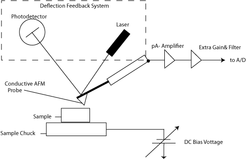
With the tip at virtual ground, a selectable bias voltage is applied between the conductive tip and sample (see Figure 1). While scanning in Contact Mode, a linear amplifier with a range of 1pA to 1μA senses the current passing through the sample. By maintaining a constant force between tip and sample, simultaneous topographic and current images are generated, enabling the direct correlation of local topography with electrical properties.

Figure 1: Conductive AFM Block Diagram
| www.bruker.com | Bruker Corporation |
| www.brukerafmprobes.com | 112 Robin Hill Rd. |
| nanoscaleworld.bruker-axs.com/nanoscaleworld/ | Santa Barbara, CA 93117 |
| Customer Support: (800) 873-9750 | |
| Copyright 2010, 2011. All Rights Reserved. |