Scanning Capacitance Microscopy (SCM) images two-dimensional carrier profiles in semiconductor devices and materials, measuring small capacitance variations with high spatial resolution.
While scanning in Contact Mode, the tip and sample form a small metal-insulator-semiconductor (MIS) capacitor. The capacitance value is monitored using a high frequency resonant circuit. By maintaining a constant force between tip and sample, simultaneous topographic and capacitive images are generated, enabling the direct correlation of local topography with electrical properties. Selectable AC and DC biases are applied between the sample and the conductive tip, with the tip acting as a virtual ground.
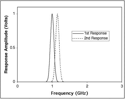
An Ultra High Frequency (UHF = 880 to 1050 MHz) resonant capacitance sensor is the basis of the capacitance detection. A resonator is formed with the MIS capacitor at the end of a transmission line. Tip-sample capacitance variations change the resonant frequency of the high-Q circuit (Q equals the resonant frequency divided by the width of the resonance at half of its peak amplitude, where resonance refers to the peak of the function of response amplitude versus driving frequency). Small changes in resonant frequency create enormous changes in response amplitude at frequencies near either the starting or the ending resonant frequency (see Figure 1). The SCM system is capable of 10–22F/√Hz sensitivity.
Figure 1: Example: Comparison of Response Amplitude at 1 GHz Between Two Nearby Resonances
A kilohertz AC bias voltage is applied to the semiconductor to induce capacitance variation in the sample (see Figure 2). The tip alternately attracts and repels free carriers beneath the tip due to the alternating electric field. This carrier behavior may be modeled as a moving capacitor plate (see Figure 3). Three quantities determine the depth of depletion and hence capacitor plate motion:
The absolute resolution is generally a few nanometers greater than the radius of the tip. Lateral resolution is dependent on the following:

Figure 2: Scanning Capacitance Microscopy Block Diagram
Scanning capacitance microscopy measures the rate of change of the MIS capacitance with change in applied voltage, dC/dV. Metal-insulator-semiconductor capacitance varies with the depletion/accumulation depth under the tip.
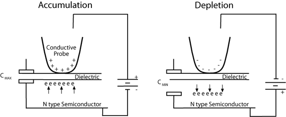
Figure 3: Change from Accumulation to Depletion During SCM Due to Alternating Electric Field
If a semiconductor surface is free of oxide, the tip/sample interface is a Schottky contact (direct metal to semiconductor contact). In this case, the physics of the interaction is more complex and current flows between the capacitor “plates.”
Figure 4 shows a typical high frequency capacitance-versus-voltage (CV) relationship for high and low concentration N-type semiconductors. For P-type material, the CV curve polarity inverts. With a positive voltage applied to the gate (the conductive probe in this case), the carriers in the material (electrons for N-type) are attracted to the surface and accumulate there. In accumulation, the capacitor plates for the semiconductor are close together and the MIS capacitance is the capacitance across the dielectric oxide. As the voltage on the gate swings negative, the electrons move away from the gate, depleting the material of carriers. This increases the spacing between the semiconductor capacitor plates and lowers the capacitance.
The lower concentration material depletes faster; hence the capacitance decreases faster with voltage. Therefore, the slope of the CV curve (or dC/dV) is larger for the low concentration.
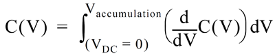
By applying a constant amplitude AC voltage, VAC, while varying the DC voltage, VDC, and measuring the capacitance across the tip/sample dielectric, the derivative of the CV curve is obtained: dC(V)/dV = DC(VDC)/VAC. Integrating determines the C(V) function:
To avoid overdriving an uncharacterized semiconductor, use Constant Depletion SCM Mode by applying feedback from the measured capacitance to the applied AC voltage to maintain a constant MIS capacitance, so a constant depletion depth.
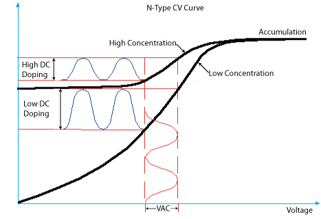
Figure 4: N-type Capacitance versus Applied AC Voltage (CV) Curves, by Carrier Concentration
| www.bruker.com | Bruker Corporation |
| www.brukerafmprobes.com | 112 Robin Hill Rd. |
| nanoscaleworld.bruker-axs.com/nanoscaleworld/ | Santa Barbara, CA 93117 |
| Customer Support: (800) 873-9750 | |
| Copyright 2010, 2011. All Rights Reserved. |