SSRM Imaging
| |
- For initial settings of the Scan and Feedback parameters in Contact Mode, refer to your instruction manual.
- Set Channel 1 > Data Type to Height Sensor, Channel 2 > Data Type to Deflection Error and Channel 3 > Data Type to Resistance. The topographic and SSRM resistance information display simultaneously.
- Set (resistance) Channel 3 > Real-Time Plane Fit and Offline Plane Fit to None.
|

|
- Click Engage to initiate tip/sample contact and start the measurement.
|
DC Sample Bias and Deflection Setpoint are the two most important parameters for SSRM imaging. A higher Deflection Setpoint corresponds to a higher force between the tip and sample. In order to obtain a stable electrical contact in SSRM, a minimum force is required. At low forces, the observed resistance values will be high (and often out of range). Upon increasing the force, the electrical contact becomes more stable, and the resistance drops to a lower, more stable value. An effective setting of Deflection Setpoint depends on the sample material and the tip used. In general, higher forces are needed for SSRM imaging of Si-based structures, as compared to other materials (e.g., metals, III-V semiconductor structures, etc.).
The optimum DC Sample Bias for SSRM imaging depends on the sample material. For Si-based and metal structures, DC Sample Bias can be small values (–0.5 V to 0.5 V), whereas compound semiconductor structures often require several volts of positive or negative sample bias. As tip contact with some samples produces non-Ohmic behavior (not according to Ohm’s Law: voltage equals current times resistance), the polarity of DC Sample Bias can have an important effect on measured values. Try different magnitudes and polarities of DC Sample Bias to optimize SSRM images. An example of simultaneously obtained topography and SSRM resistance images of a cross-sectioned silicon DMOS transistor show differently doped regions in Figure 1.
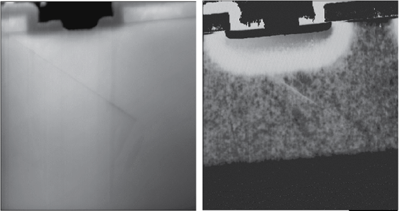
Figure 1: 12 micron scan SSRM Topography (left), Resistance (right) Images of a DMOS Transistor
Resistance data is provided in units of volts. Because a logarithmic amplifier is used, a one volt change corresponds to a resistance change of one order of magnitude. One megaohm (1 MΩ) resistance corresponds to 0 V output, independent of the applied bias voltage. The relation between output voltage, Vout, and input current, I, is:
- Vout = sign(Vbias) * log (I * 106/Vbias), where
- sign(Vbias) = +1 if Vbias > 0 and
- sign(Vbias) = –1 if Vbias < 0, (see Figure 2)
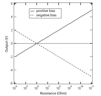
Figure 2: Transfer Curve of the SSRM Logarithmic Current Amplifier
| www.bruker.com
|
Bruker Corporation |
| www.brukerafmprobes.com
|
112 Robin Hill Rd. |
| nanoscaleworld.bruker-axs.com/nanoscaleworld/
|
Santa Barbara, CA 93117 |
| |
|
| |
Customer Support: (800) 873-9750 |
| |
Copyright 2010, 2011. All Rights Reserved. |
Open topic with navigation