Scanning Spreading Resistance Microscopy (SSRM) extends the range of tip/sample currents tolerated by the TUNA Application Module to measure sample surface resistance. SSRM measures the resistivity (the reciprocal of conductivity) of samples spanning a wide range of conductivity, from insulating through semiconducting to metallic. SSRM is especially useful in two-dimensional mapping of electrical carriers in semiconductors.
The geometry of the tip determines the lateral resolution, which is roughly equal to the end radius of the tip. With the tip at virtual ground, a selectable bias voltage, VDC, is applied between the conductive tip and sample. While scanning in Contact Mode, a logarithmic current amplifier with a range of 10 pA to 0.1 mA senses the current, I, passing through the sample. Resistance is calculated from Ohm’s Law: R = VDC/I. Material resistivity, in ohm-meters, is defined as the resistance times the cross-sectional area divided by the length of the conducting path made of the material. By maintaining a constant force between tip and sample, simultaneous topographic and current images are generated, enabling the direct correlation of local topography with electrical properties.
The resistance measured is the sum of contact resistance at the tip/sample interface plus the spreading resistance radially from the point of contact plus the bulk resistance along the path(s) completing the circuit to the conductive platform supporting the sample. To reduce the material-independent contribution of contact resistance to the total resistance measured, contact area cannot be appreciably increased without losing spatial resolution, so contact force is increased above the minimum necessary to maintain contact. For instance, on silicon, a few micronewtons of force, combined with a low sample bias voltage (e.g., between –1 V and 1 V) provide a consistent low contact resistance while scanning the surface of most compound (such as InP- and GaAs-based) semiconductor structures. Where a lower force is required (to avoid tip/sample wear), increase the bias by several volts. For an ideal circular, Ohmic contact, the spreading resistance is R = r/4r, where r is the local sample resistivity and r is the radius of the contact.
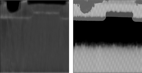
A sample SSRM image is shown in Figure 1.
Figure 1: SSRM Image of a Silicon-based MOSFET (5 µm Scan)
| www.bruker.com | Bruker Corporation |
| www.brukerafmprobes.com | 112 Robin Hill Rd. |
| nanoscaleworld.bruker-axs.com/nanoscaleworld/ | Santa Barbara, CA 93117 |
| Customer Support: (800) 873-9750 | |
| Copyright 2010, 2011. All Rights Reserved. |