Sample Preparation
In some situations, the sample volume of interest is not at a surface. Cross-section a sample to expose the interior at a visible surface. A procedure for preparing finely polished sample cross-section surfaces follows. SCM and SSRM samples are discussed explicitly because these more often require cross-sectioning. The procedures may just as well be applied to cross-sectioning TUNA and C-AFM samples. An animated sample preparation procedure is available from Bruker upon request.
For 2-D carrier profiling, the region of interest must be accessible to the profiling instrument. If this region is below the sample surface, a cross-section of the sample is required. Preparation of semiconductor cross-sections usually involves cleaving and/or polishing. The most important criteria for a cross-section surface are: low roughness, cleanliness and no surface damage. This portion of this manual overviews possible sample preparation techniques employing a diamond saw, a lapping apparatus and silver epoxy. It may be necessary to apply a sputtered coating. In general, standard electron microscopy techniques for sample preparation work well, though the surface finish required is more exacting for SCM and SSRM. The following technique may be carried out and a sample prepared within a few hours with a little practice.
Sample Preparation Equipment
- N2 dry box
- Hot plate
- Nikon Optihot-100 with 10X or 20X wide field eyepieces
- 5X, 20X and 50X Bright field / Dark field / Differential Interference Contrast (BF, DF, DIC plan Apo) objectives
- 100X or 150X plan Apo BF/DF objective
- Stereo zoom scope (Nikon SMZ-2 + ring light and stand)
- Buehler Ecomet 3 or 4 polisher
- Ultraviolet (UV) light source (wavelength below 300)
Consumables
- Cross-section holder (e.g., Allied Hightech PN 69-30000)
- Glass slides
- Epoxy (e.g., Epoxy bond 110 Allied PN 71-10000)
- Silver epoxy (e.g., Dynaloy PN 325 A/B)
- Silver paint (e.g., Ted Pella #16035)
- Replication tape (e.g., Ted Pella #44841)
- Diamond Lapping Films (e.g., 0.1, 0.5, 1, 6 and 15µm, Buehler PN 15-7691, 6795, 6801, 6807, 6815, respectively)
- Diamond suspensions for Texmet 0.1, 0.25µm, Buehler PN 40-6528, 6529, respectively
- Texmet 1000 polish pad, Buehler PN 40-7618
Cross Section Sample Preparation
SCM and SSRM cross section preparation steps are listed below and represented in Figure 1.
- Cement semiconductors of interest into a stacked “sandwich” using G1 epoxy or equivalent.
- Press the pieces together to remove all air bubbles.
NOTE: Glass plates may be epoxied to the bottom and top of the sandwich to strengthen and protect the semiconductors within.
- Allow the epoxied stack to heat cure thoroughly.
- Use a diamond saw to slice off approximately 0.5mm of the semiconductor sandwich.
NOTE: Do not sputter coat onto the polished surface to be imaged.
- For optimal electrical contact, sputter the semiconductor stack with gold where it will contact the puck or stage of the SPM.
- Using silver epoxy or a low temperature wax, attach the mounting side of the sample to the underside of a polishing fixture. Spread the coating evenly to provide a broad contact area.
- Install the loaded fixture on a lapping plate.
- Polish the semiconductor sandwich to expose the region of interest. Verify that the sample is polished flat to a root mean square (RMS) roughness of <0.2nm to produce a superior image.
- By irradiating it with UV light, reduce the conductivity of the surface silicon oxide film that forms:
- Place the sample on a hot plate at about 200-300ºC for 20 minutes of which 1 minute includes high-intensity UV radiation.
NOTE: This preparation step results in a surface which shows no Fermi-level pinning and only a moderate density of surface electronic states.
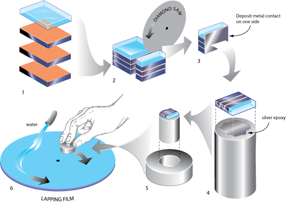
Figure 1: SCM and SSRM: Semiconductor Cross-Section Preparation
Details of the Polishing Procedure
NOTE: When polishing, maintain a small, constant downward pressure against the lapping plate while moving the fixture in small, counter-clockwise circles.
- Rotate the lapping plate at 90-120 rpm.
- Starting with 10µm diamond grit paper, lap the sample until achieving a uniformly flat surface; remove all traces of the saw cut.
- Use 3µm diamond paper, remove approximately 30µm.
NOTE: Before proceeding to a smaller grit remove a thickness of sample material at least three times the particle size of the lapping compound in use. A typical sequence of diamond particle lapping papers to use for achieving a highly polished surface is:
- 10-micron: to remove saw grinding marks and smooth the sample
- 3-micron: polish for 5 minutes
- 1-micron: polish for 5 minutes
- 0.5-micron: polish as needed
- 0.1-micron: polish as needed
- Remove the surface damage left by the diamond paper process by using a colloidal diamond slurry. To avoid contamination, use a new polish pad dedicated to one grit (e.g., napless cloth). The following lapping order gives good results:
- 1-micron : polish for 5 minutes
- 0.5-micron: polish for 10 minutes
- 0.25-micron: polish for 20 minutes
- 0.1-micron: polish as needed
- Use 0.05-micron colloidal silica for the final cleaning and polishing of the sample surface. Apply for 15-30 seconds. Run clean water for at least 30 seconds.
- Clean the sample surface with a swab and soapy running water, then wipe or blow dry.
- If a powered lapping plate is unavailable, lap and polish the sample on a stationary flat surface by moving the fixture and ring in small figure-eight motions while periodically rotating the fixture within the ring to ensure even abrasion.
NOTE: Be certain to keep the fixture and lapping surface (plate or paper) wet, and always clean them completely before switching to a smaller grit.
NOTE: The most important tools in polishing are patience and a good optical microscope for inspection of the sample surface—e.g., with bright field, dark field and differential interference contrast combined objectives in magnifications of 5X, 20X and 50X.
- When grinding and polishing are complete, clean the sample thoroughly using water and wipe or blow dry.
Sample Cleaning Procedure
Surface water layers, ionic residue and charges trapped in surface oxide all introduce anomalous conditions to a sample that can distort SCM and SSRM images. Introduced charges offer unrepresentative conductive paths which lower the apparent resistance of an SSRM sample. Because SCM applies a local field between tip and sample and measures the response of carriers to that field, extraneous charge may create a field that counteracts the applied field, nulling the capacitive effect. This appears as a loss of contrast or variation in the expected sample response. Due to the geometry of the tip/dielectric/silicon of the samples, a local packet of charge can produce a localized effect equivalent to many volts of applied field either pinning the carriers at the surface or depleting the surface of free carriers. Each of these charge effects destroy contrast in an SCM image, so it is worthwhile to remove such charges. Both positive and negative charges may become trapped in surface oxide by applying too large a bias voltage—enough to cause current flow (± 8V). Mobile surface charges such as sodium and potassium ions, contaminants usually introduced in skin oil through handling, diffuse into surface oxide. Extraneous charge can be hard to remove, so it is better to prevent its introduction through conservative application of bias voltage and only handling samples with clean tweezers.
WARNING: Do not allow skin contact with surfaces of interest for SCM and SSRM imaging. Only handle samples with clean tweezers. Store samples in a nitrogen atmosphere and/or desiccated dry box, particularly in a humid climate. Preferred cleaning processes provide a hydrophobic (water repelling) surface on the oxide.
Replicating Tape After UV Light Baking
WARNING: Clean samples with solvents only in a well-ventilated area. Generally avoid skin contact with solvents. With acetone, particularly avoid contact with mucous membranes, such as around eyes. Dispose of all wipes and swabs properly.
- Cover the sample with a spray of clean acetone.
- Set a square of acetate replicating tape over the surface.
NOTE: Replicating tape, commonly used in electron microscopy, partially dissolves in the acetone and then dries and adheres tightly to the sample surface. As you peel back the tape, sample surface contaminants adhere to it. The tape may also be left on the sample as a protective coating until you are ready to image it.
Colloidal Silica
A second cleaning method is more sophisticated: passivate the surface with an alkali solution found in a common Chemical-Mechanical Polishing (CMP) compound.
- Wipe the sample with either acetone or alcohol to remove oils. Next apply a standard non-crystallizing 0.05µm colloidal silica suspension to the sample surface and rub it around with a swab.
- Rinse the silica suspension off with deionized water.
- Use a few drops of soap and another swab to clean the surface of the silica particles.
- Rinse the sample again in deionized water and blow dry from one edge, with clean filtered air or nitrogen.
NOTE: The silica method may be more effective than replicating tape against a charge layer on the sample surface.
| www.bruker.com
|
Bruker Corporation |
| www.brukerafmprobes.com
|
112 Robin Hill Rd. |
| nanoscaleworld.bruker-axs.com/nanoscaleworld/
|
Santa Barbara, CA 93117 |
| |
|
| |
Customer Support: (800) 873-9750 |
| |
Copyright 2010, 2011. All Rights Reserved. |
Open topic with navigation