 .
.Etched silicon probes provide the most consistent tip sharpness of the probes presently available. Because they are sharper, etched silicon tips provide better resolution and have less applied capillary forces.
There are subtleties in general shape that produce certain effects when imaging samples with steep walls over steps of 100 nm to several micrometers in height (see Figure 1, below).
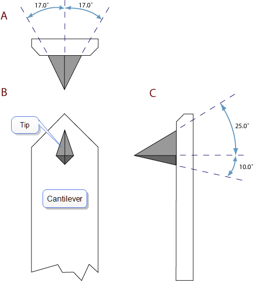
Figure 1: Theoretical tip shape of silicon probes
The present process creates a tip that is symmetric from side-to-side with a 17 ± 2° half cone angle (see A in Figure 1, above) and asymmetric from front-to-back, along the length of the lever (see C in Figure 1, above).
The substrate mounting angle also affects the interaction of the tip shape with the surface. Along the front edge of the tip, the half angle is nominally 25°, while at the back edge of the tip, the half angle is approximately 10°. Neither of these angles account for the tilt of the substrate. With the mounting angle of the substrate factored in, the front edge of the tip is 35° and the back edge of the tip is zero degrees. From the tip side, the cross-section of the tip near the lever is approximated by an inverted ‘kite’ shape. All of these subtleties arise from the etching process used to make the tip, which employs caustic solutions to perform wet anisotropic etching of the silicon.
The effects of this tip geometry are illustrated in Figure 2 and Figure 3, below.
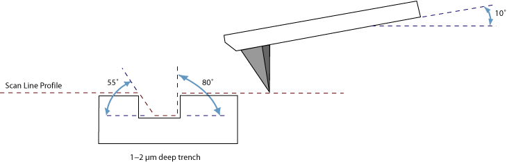
Figure 2: Scan line produced using a theoretical probe tip shape on a 1–2 µm deep vertical wall trench (front-to-back tip profile artifact)
To measure sidewall angles, the best orientation of the sample uses the back edge of the tip (which faces back towards the cantilever substrate) to measure step angles (see Figure 2, above). Using the back edge, step angles approaching 90 degrees can be measured routinely, depending on the step height. Any wall imaged by the front edge (left, in Figure 2) that is greater than 55 degrees will appear as 55 degrees in the image.
This method does not work well in small openings of less than 5 micrometers where, depending on the depth of the step, other tip edges may contact other faces of the small opening. Wall angle measurements are best measured in open areas for these reasons.

Figure 3: Scan line produced using a theoretical probe tip shape on a 1–2 µm deep vertical wall trench (side-to-side step profile artifact)
Measurements of line pitch are often best measured using the side-to-side faces of the tip, which exhibits symmetry. Because of the approximate 17° half angle of the tip, the line or space measurement is best done at the top of the line for simplification of the measurement artifacts (see Figure 3, above). Any wall angle that is greater than 73 degrees will appear as 73 degrees in the image.
Figure 4 depicts the resultant effect of the angled back ridge on the step angle measurement for a deeper trench depth. This is tip and topography dependent:

Figure 4: Subsequent scan line produced using the realistic probe tip shape (resultant scan artifact of a common silicon probe)
Figure 4 above depicts the resultant effect of the angled back ridge on the step angle measurement for a deeper trench depth. This is tip and topography dependent.
In addition to microscopic-scale shape characteristics in the figures above, another factor that can affect the wall angle over shorter (nominal 100 nm) step height measurements is the shaped cusp at the end of the tip. The shaped cusp at the end of the tip is formed to increase the sharpness of the tip point to a length of 100 nm from the end of the tip. It is formed in such a manner that the radius of curvature of a silicon tip can be in the range of 5–10 nm (on a very good tip).
| www.bruker.com | Bruker Corporation |
| www.brukerafmprobes.com | 112 Robin Hill Rd. |
| nanoscaleworld.bruker-axs.com/nanoscaleworld/ | Santa Barbara, CA 93117 |
| Customer Support: (800) 873-9750 | |
| Copyright 2010, 2011. All Rights Reserved. |
 Related Topics