 .
. Silicon nitride probes are low cost and durable probes suitable for Contact AFM imaging. Each silicon nitride cantilever substrate includes 4 cantilevered tips with different size and spring constants.
There are some subtleties in general shape that should be understood to gain the best advantage from the silicon nitride tips when imaging samples with steps of 0.1 to several micrometers in height. The probe tip is approximated by a pyramid formed by intersecting <111> planes in silicon. The approximate shape of the tip is shown in Figure 1 below along with dimensions and approximate values for the cantilevers' spring constants and resonant frequencies.
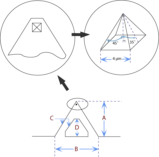
| Lever Type | A | B | C | D | Spring Constant (N/m) | Measured Frequency (kHz) |
|---|---|---|---|---|---|---|
| 100 µm Wide | 115 | 122 | 21 | 60 | 0.58 | 40 |
| 200 µm Wide | 193 | 205 | 36 | 113 | 0.12 | 12.3–22.1 |
| 100 µm Narrow | 115 | 122 | 15 | 69 | 0.38 | – |
| 200 µm Narrow | 193 | 205 | 20 | 150 | 0.06 | – |
Figure 1: Silicon nitride cantilever specifications (A, B, C, and D in the table refer to dimensions in Figure 1)
Cantilevers with smaller spring-constants are used on softer samples, which are destroyed by imaging with high-contact forces. The tabulated values above are used to approximate contact force, unless more accurate values are measured by the user.
Because the Silicon Nitride probe tips have lower aspect ratios than single-crystal etched silicon probes, the steepest measurable step wall angle is appreciably lower. The highest measurable angle using silicon nitride probes is approximately 65° (see Figure 2, below) using the inner face of the tip (towards the cantilever holder). The steepest measurable angle from side to side (parallel to the edge of the probe's substrate) is approximately 55°. Both of these figures assume that the measurement does not have interference from other edges.
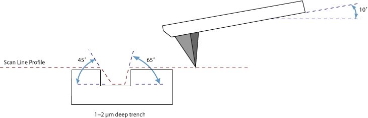
Figure 2: Silicon nitride cantilevers (profile)
There are two types of silicon nitride cantilever probes available: standard and oxide-sharpened tip processes. The standard devices have the nitride deposited directly into the etched silicon mold pit formed by the intersecting <111> planes, and have points that are slightly rounded with respect to the tips produced using the oxidation sharpening process.
The oxide-sharpened silicon nitride probes have a thermally grown silicon dioxide film deposited in the mold pit used to shape the nitride tip, prior to silicon nitride film deposition. The oxide has two effects: it shapes the inner contours of the pyramidal pit so that a slight cusp forms at the point of the pyramid, and the oxide protects the tip from excessive exposure to a long duration wet silicon etch used to free the cantilevers from the silicon substrate. The result is a noticeably sharper point at the end of the pyramid. Regrettably, along with the increased sharpness of the tip comes a slight increase in double tip effect experienced with the oxide sharpened process.
| www.bruker.com | Bruker Corporation |
| www.brukerafmprobes.com | 112 Robin Hill Rd. |
| nanoscaleworld.bruker-axs.com/nanoscaleworld/ | Santa Barbara, CA 93117 |
| Customer Support: (800) 873-9750 | |
| Copyright 2010, 2011. All Rights Reserved. |
 Related Topics