Power Spectral Density (PSD)

|
The Power Spectral Density (PSD) function is useful in analyzing surface roughness. This function provides a representation of the amplitude of a surface’s roughness as a function of the spatial frequency of the roughness. Spatial frequency is the inverse of the wavelength of the roughness features.
|
The PSD function reveals periodic surface features that might otherwise appear random and provides a graphic representation of how such features are distributed. On turned surfaces, this is helpful in determining speed and feed data, sources of noise, etc. On ground surfaces, this may reveal some inherent characteristic of the material itself such as grain or fibrousness. At higher magnifications, PSD is also useful for determining atomic periodicity or lattice.
PSD and Surface Features
The synthetic surface represented in Figure 1 consists of essentially two dominant wave forms: a long period waveform along the X-axis, and a shorter period waveform along the Y-axis.

Figure 1: Wavelength Depiction
A 2-dimensional power spectral density plot of this surface would consist of two dominant spikes (one for each dominant wavelength), plus some number of extra wavelengths inherent within the image. (These extra wavelengths may appear due to fine surface features and/or side bands of the dominant wave forms.)
Because of the sinusoidal nature of the composite wave form, a relatively small set of spectral frequencies suffices to describe the entire surface. By contrast, an image comprised of angular (saw-toothed or square) waveform contains more spatial frequency components.
PSD and Flatness
PSD is used increasingly as a metrology tool for evaluating extremely flat surfaces, such as polished or epitaxial silicon. Generally, the desired surface is expected to adhere to certain PSD thresholds, signifying it meets a specified flatness criterion.
The main advantage gained over traditional RMS specifications is that PSD flatness is qualified through the full spectral range of interest. For example, one may specify spectral thresholds at frequencies measured on the atomic scale, thus ensuring surfaces consist largely of uniform lattices. Setting the precise thresholds for various materials remains a matter of debate.
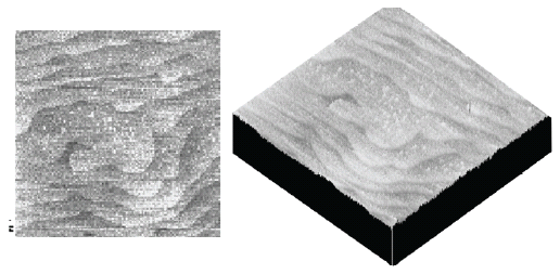
Figure 2: Epitaxial Gallium Arsenide
This surface above is comprised of “terraces” formed from the material’s natural lattice structure; each terrace is one atomic monolayer thick and is spaced at fairly regular intervals. This degree of flatness is handily evaluated with PSD, as the terraces produces a spectral spike corresponding to their spacing wavelength.
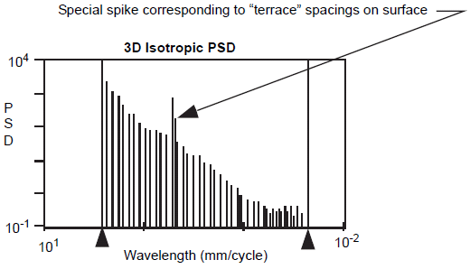
Figure 3: PSD Analysis of Epitaxial Gallium Arsenide
This tapered PSD plot is characteristic of flat, isotropic surfaces. Longer wavelengths are present up to the scan width, and are accompanied by uniformly decreasing powers of shorter wavelengths down to 2 pixels. On the plot shown above a spike stands out, corresponding to the wavelength spacing of the terraced features. Depending upon the qualitative standards of the person evaluating such a plot, this spike may exceed a threshold standard of flatness.
PSD Algorithm
Over a given range of spatial frequencies the total power of the surface equals the RMS roughness of the sample squared.
The frequency distribution for a digitized profile of length L, consisting of N points sampled at intervals of do is approximated by:
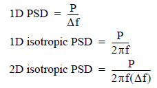
Where frequencies, f, range from 1/L to (N/2)/L. Practically speaking, the algorithm used to obtain the PSD depends upon squaring the FFT of the image to derive the power. Once the power, P, is obtained, it may be used to derive various PSD-like values as follows:
The terms used in the denominators above are derived by progressively sampling data from the image’s two-dimensional FFT center.
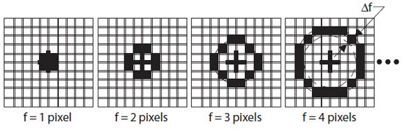
Figure 4: Progressive Data Sampling
Each sampling swings a “data bucket” of given frequency f. Since samples are taken from the image center, the sampling frequency, f, is limited to (N/2)/L, where N is the scan size in pixels. This forms the upper bandwidth limit (i.e., the highest frequency or Nyquist frequency) of the PSD plot. The lower bandwidth limit is defined at 1/L.
Power Spectral Density Procedure
| |
- Select an image file from the file browsing window at the right of the main window. Double-click the thumbnail image to select and open the image.
- You can open the Power Spectral Density view, shown in Figure 6, using one of the following methods:
- Right-click on the image name in the Workspace and select Add View > Power Spectral Density from the popup menu. See Figure 5.
|
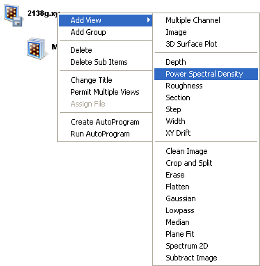
Figure 5: Select Power Spectral Density from the workspace
| |
Or
- Right-click on a thumbnail in the Multiple Channel window and select Power Spectral Density.
Or
- Select Analysis > Power Spectral Density from the menu bar.
Or
|
|
|
- Click the Power Spectral Density icon in the NanoScope toolbar.
|
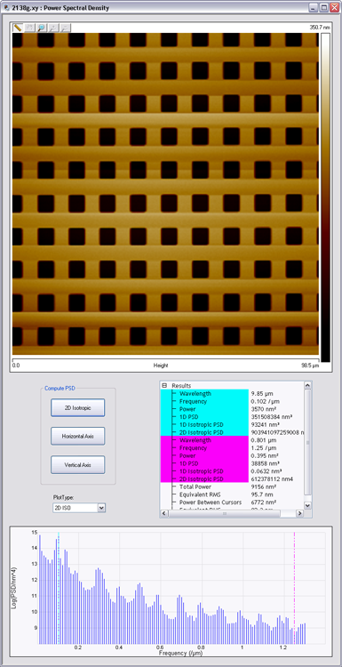
Figure 6: The PSD Analysis Window
PSD Interface
Compute PSD Buttons
Once the PSD analysis window is opened, select the type of spectral density analysis you wish to perform by clicking the appropriate button in the Compute PSD window.
- 2D Isotropic—Executes a two-dimensional PSD analysis.
- Horizontal Axis—Executes a one-dimensional PSD analysis along the X-axis.
- Vertical Axis—Executes a one-dimensional PSD analysis along the Y-axis.
The calculation begins as soon as one of these buttons is selected. The PSD and a table of values from the graph are shown in the Results window. Completion of the analysis will also result in a topographical histogram in the spectrum plot window, shown in Figure 7.
Results Display
The Results window displays the Name and Value of the procedures performed during a PSD analysis. The teal shaded area in the display window corresponds to the area designated by the teal cursor on the Power Spectral Density histogram, and the magenta shaded area corresponds to the magenta cursor. You can generate a report by right-clicking in the Results window, selecting Copy Text and pasting the clipboard into another application (e.g. Notepad, Word...).

Figure 7: PSD Results
| Parameter |
Description |
|
Wavelength
|
The wavelength at current cursor positions. See λx and λy in Figure 1. |
|
Frequency
|
The spatial frequency, 1/(λ), at current cursor positions. |
|
Power
|
Power measured in nm2 at current cursor positions. |
|
1D PSD
|
One-dimensional power spectral density measured in nm3; P/(Δf) |
|
1D Isotropic PSD
|
One-dimensional isotropic power spectral density measured in nm3; P/(2πf) |
|
2D Isotropic PSD
|
Two-dimensional isotropic power spectral density measured in nm4; P/2πf(Δf) |
|
Total Power
|
The sum of the power contained in the entire spectrum. |
|
Equivalent RMS
|
The root mean square (RMS) roughness of the sample. It is calculated as the square root of the total power. |
|
Power Between Cursors
|
The sum of the power contained in the portion of the spectrum between the cursors. |
|
Equivalent RMS
|
The root mean square (RMS) roughness of the sample contained by the frequencies between the cursors. It is calculated as the square root of the integral of the power between the cursors. |
Table 1: Results Parameters
Select Displayed Parameters
The operator can select which Results will or will not be displayed in the Results window by Right-clicking in the Results window, selecting Show All from the popup menu, and checking or un-checking the appropriate boxes. See Figure 7.
Exporting Text
Selecting Copy Text from the popup menu will copy the text from the Results window, in tab-delimited text format, to the Windows clipboard. You may then paste it into a text or word processing program.
Changing Parameters of the Spectrum Plot
The Spectrum Plot window displays results of the PSD analysis. The window has two cursors whose color corresponds to the shaded areas in the Results window. Move either of the cursors within the Spectrum Plot window by placing the cross hair cursor directly over the cursor, clicking and holding the left mouse button, and dragging the mouse to the left or right. Both cursors can be moved simultaneously by left-clicking the mouse with the cross hair cursor anywhere between the two cursors and dragging to the left or right.
To change the parameters of the Spectrum Plot, right-click in the Spectrum Plot window at the bottom of the display and choose from the popup menu. See Figure 8.
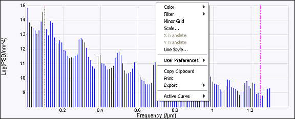
Figure 8: Spectrum Plot Window, Right-click to Change Parameters
| Parameter |
Description |
|
Color
|
Changes the colors of the curves, text, background, grid lines, minor grid lines (if selected), and the marker pairs.
|
|
Filter
|
Selects Filter type and points.
|
|
Minor Grid
|
Shows/hides minor grid lines. |
|
Scale
|
Sets the vertical axis range, the center of the range, or allows the software to autoscale. See Figure 9. |
|
Line Style
|
Changes the line style of the Spectrum Plot graphical display. See Figure 10.
Settings:
- Connect
- Fill Down
- Point
- Circle
- Square
- Triangle
- Diamond
- Cross
|
|
User Preferences
|
You can either save all changes made to the graphical display, or Restore previously saved settings. Save will result in all graphical displays maintaining any design changes made to this display. |
|
Copy Clipboard
|
Copies the graphical display only to the Windows clipboard, allowing it to be pasted into any compatible Windows program. |
|
Print
|
Prints the graphical display only to a printer. |
|
Export
|
Saves the graphical display as a JPEG graphic, a Bitmap graphic, or as an XZ Data file text, which can be read in a database program (e.g. Excel). |
|
Active Curve
|
Changes the curve displayed when more than one curve has been plotted. (Does not occur in PSD). |
Table 2: Spectrum Plot Popup Menu items
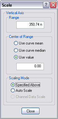
Figure 9: Scaling Menu
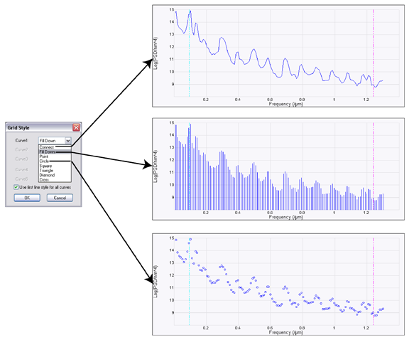
Figure 10: Line styles
| www.bruker.com
|
Bruker Corporation |
| www.brukerafmprobes.com
|
112 Robin Hill Rd. |
| nanoscaleworld.bruker-axs.com/nanoscaleworld/
|
Santa Barbara, CA 93117 |
| |
|
| |
Customer Support: (800) 873-9750 |
| |
Copyright 2010, 2011. All Rights Reserved. |
Open topic with navigation