Albanova Nano-Fab-Lab, SPM/AFM
Surface potential measurement
Some very short notes on how to measure surface potential with the
Multimode and the Nanoscope IV controller.
More info can be found in the manual for the Nanoscope IV controller.
Please note that the "main" manual refers to the Nanoscope III
controller when describing how to measure surface potential.
Using Nanoscope software Version 6.
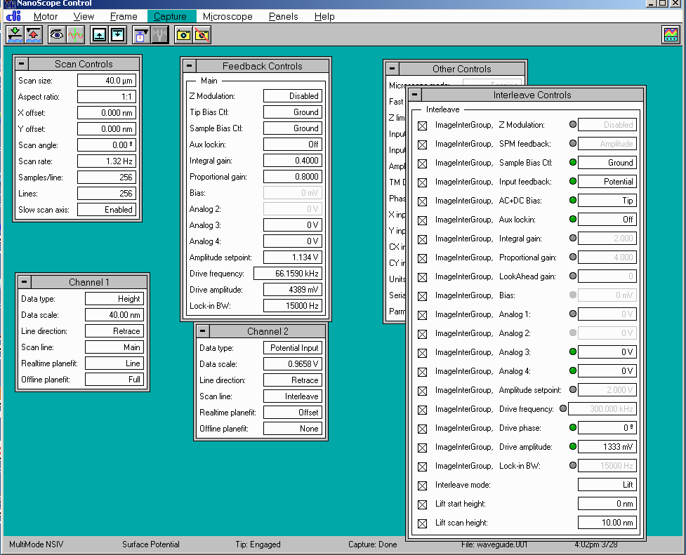
Important settings:
- Use conductive cantilever and tip (e.g. MESP)
- Set up for normal tapping mode
- Use Autotune
- Interleave must be active
- Interleave Mode must be Lift
- Input Feedback for Interleave Mode must be Potential
- AC+DC Bias should be Tip
- AC+DC Bias can be Sample, gives contrast inversion
- Start with Drive Amplitude around 6000 mV
- When Input Feedback is Potential you can select Channel 2 to
Potential.
- Set Channel 2 Data Type to Potential
- Set Channel 2 Scan Line to Interleave
- Data scale should be about 1 V for Channel 2
- Lift Start Height should be set to zero
- Lift Scan Height should start with 100 nm,
then carefully decrease
to maybe below 10 nm to get good potential imaging.
If this is not done with care the tip will probably break.
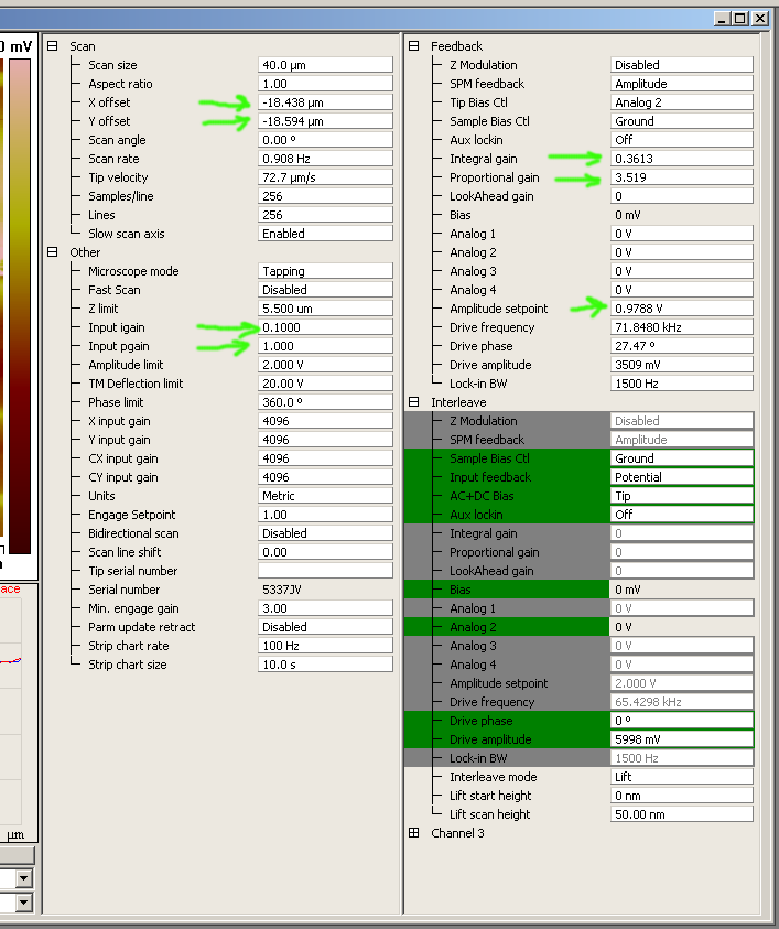
Parameters marked with green arrows should be observed and/or tweaked
for best performance.
- X- andf Y-offsets should initially be set to zero
- Input igain recommended to be 0.1
- Input pgain recommended to be 1.0
- Integral gain should be adjusted for best overlap between
Trace and Retrace scans, too high can give self-oscillations
- Proportional gain should be about ten times larger that Integral gain,
also adjust for best overlap between
Trace and Retrace scans, too high can give self-oscillations
-
Amplitude setpoint usually always has to be reduced 5-10% after initial contact.
This will give much better surface topography and better
overlap between
Trace and Retrace scans
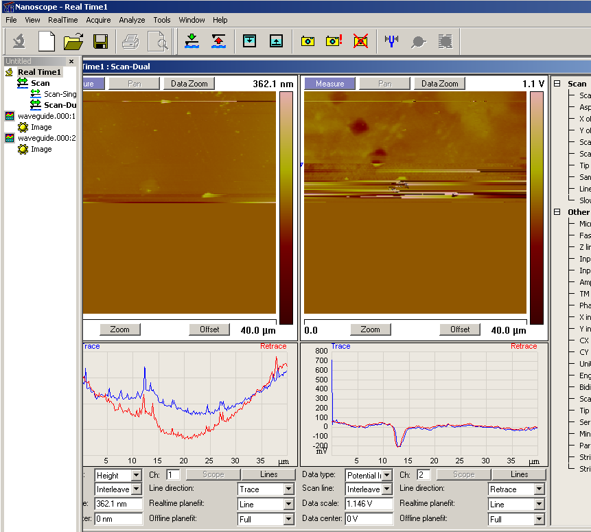
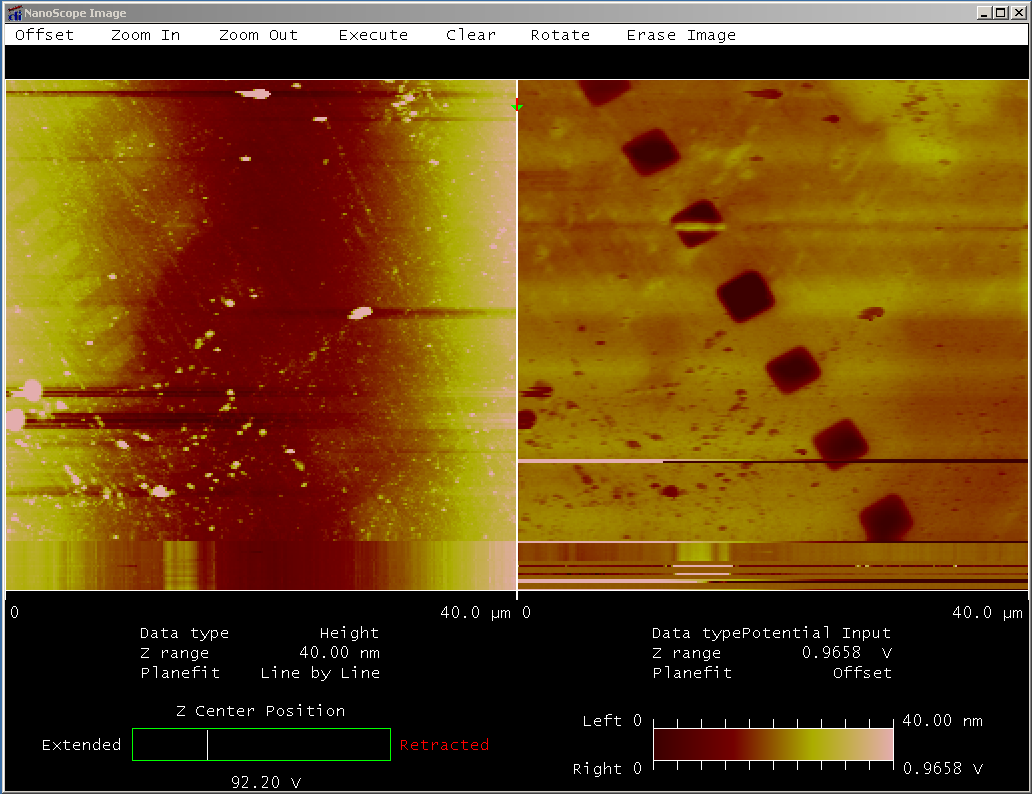
This is a waveguide made in KTP-crystal, squares have different potential
due to Potassium atoms replaced with Rubidium atoms.
This is roughly the same settings for Nanoscope software version 5.
This is a more complete image scanned with version 5.
Note that surface height does not show any change where the
potential variations are.
Note also a smaller waveguide that does not have surface potential
variations to the middle left in the height (left) image.
NanoFabLab, KTH
Anders Liljeborg