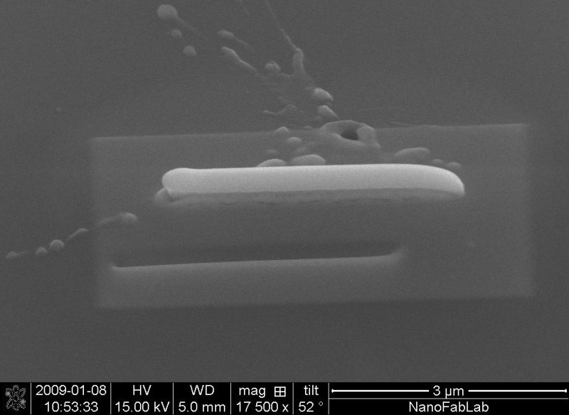
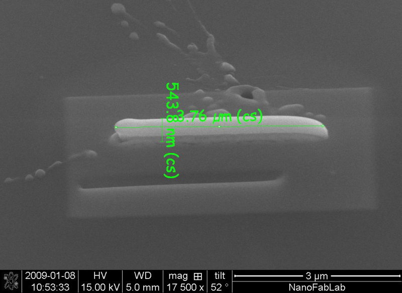
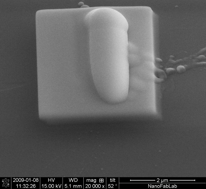
The irregular "splatter"-like structure is remnants from a Si-particle that was moved away by the bombardment of the ion beam during the start of this session.
There are also some pictures from practice of milling and depositioning of Platinum. The material is a plain Si-chip with one micron of Si-oxide.
Here are some animations.
Here a thin trench has been milled at the lower part of the picture.
Then the same milling pattern (a thin rectangle) has been used to deposit
about 0.5 µm of platinum at the center of the image.
On top of that a very thin layer of platinum (about 0.02 µm) has been
deposited over a larger rectangular area.
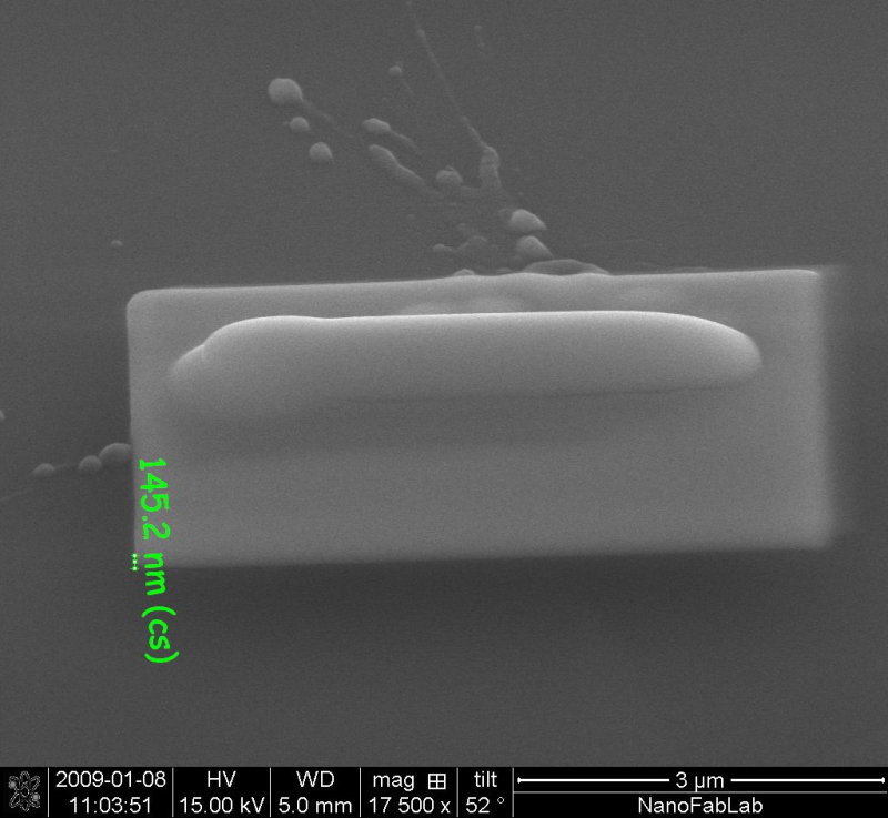
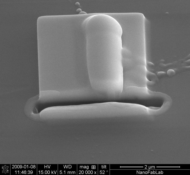
Here the same sample has been rotated 90° and tilted again to
the standard 52° (perpendicular to the ion-beam). The idea is to do
cross-sections across the Platinum-"ridge".
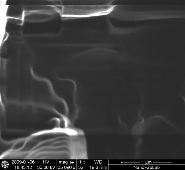
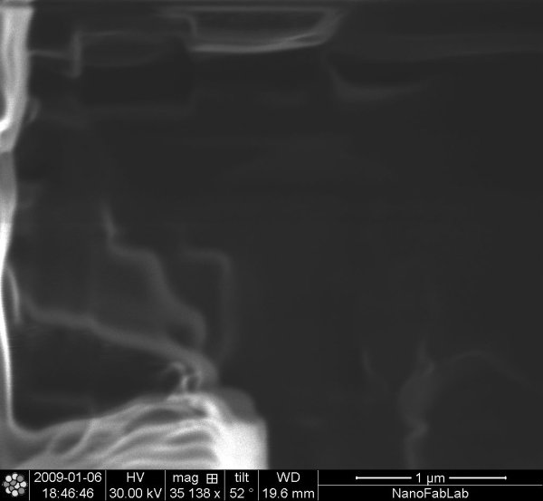
Please note the drift present during the deposition of the large area of
0.1 µm Platinum, the edges are slanting to the left.
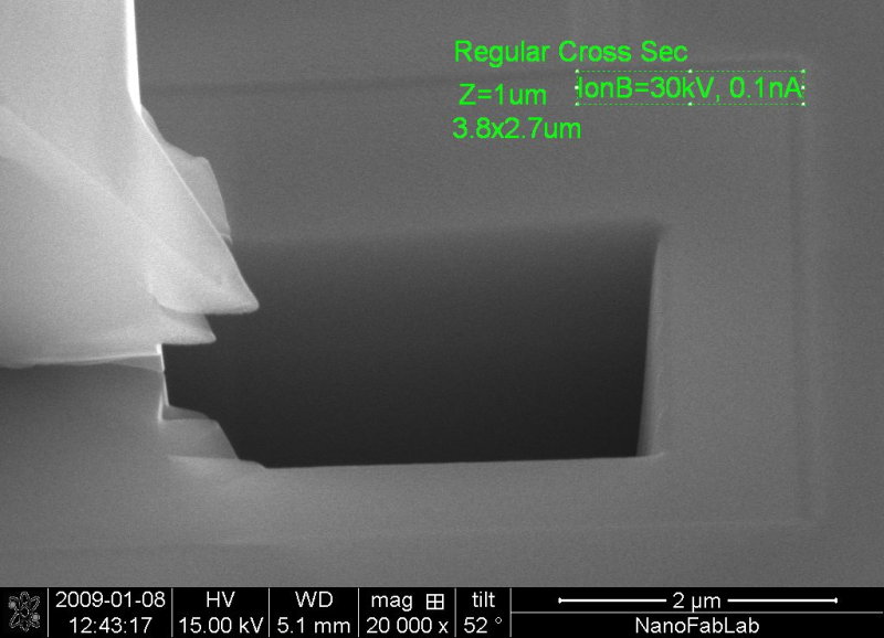
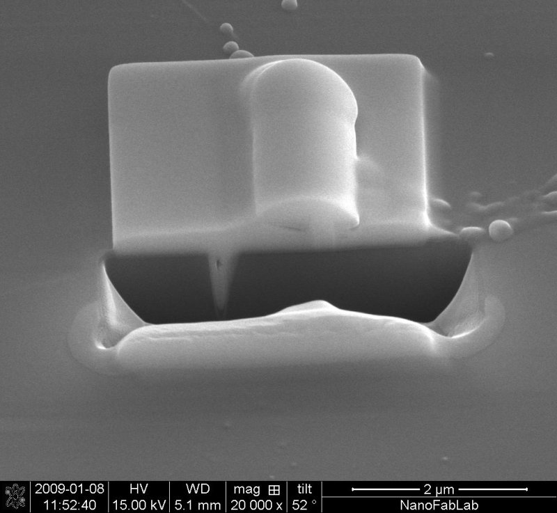
Here is a first attempt to make a "Cleaning Cross Section". The parameters for it was not good, it was too short along the vertical direction.
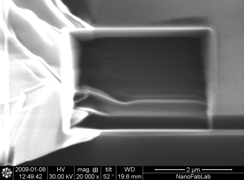
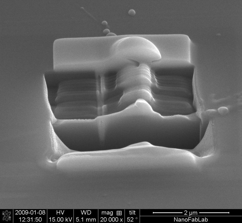
Here is a longer Cleaning Cross Section, about one micron vertical. Note the cross section through the trench filled with deposited Platinum at the left part of the cross-section.
Here is after an ASV-session has been completed. The slice depth was only 0.1 µm, only the top has been sliced through. This small slice depth was chosen to collect the series quickly, and is not representative for a proper cross section series.
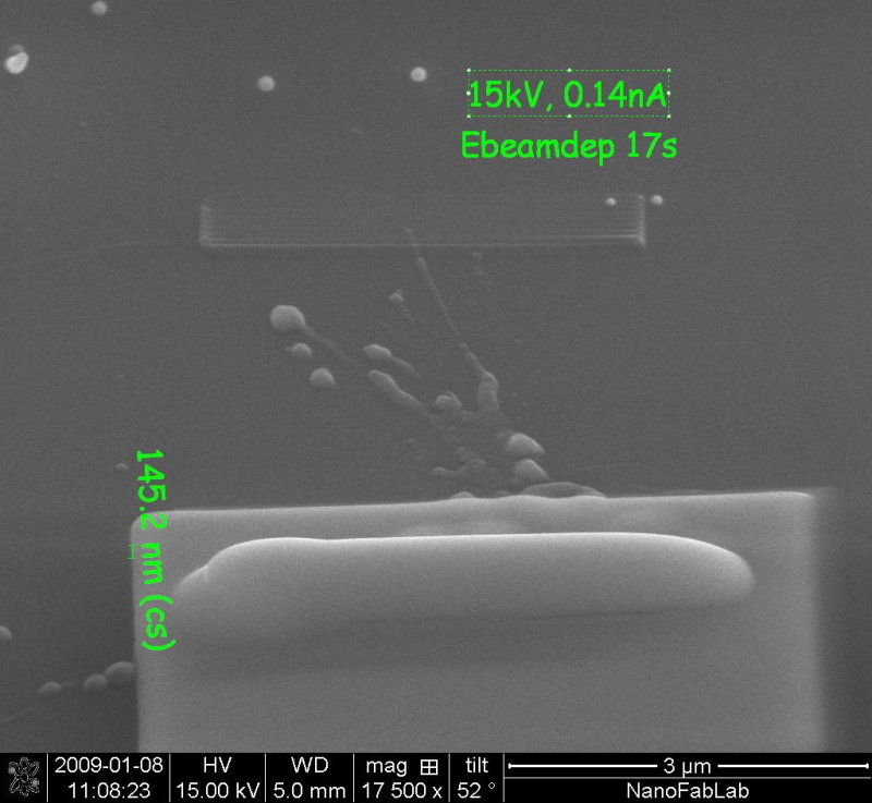
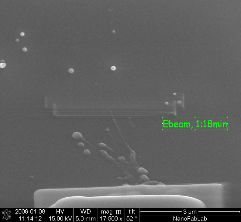
Here a second trial was done at a longer time, although there is not
much difference. Still the same thin strips of deposited material.
It could be that the smaller width of the e-beam was not taken into account,
i.e. same step size was used as when depositing with the ion-beam.
Note that these depositions are done at 52° tilt.
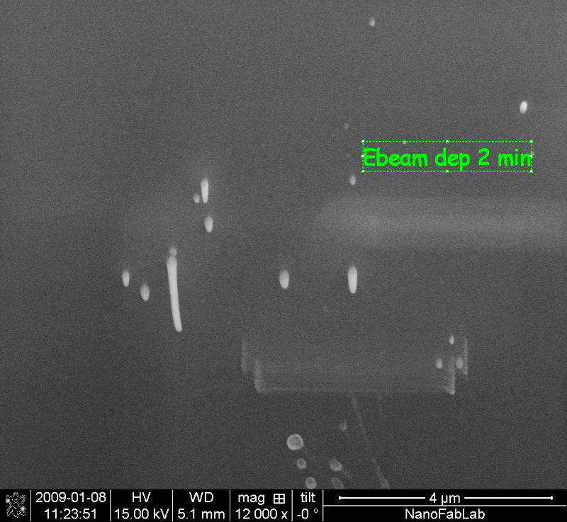
Here the sample is at zero tilt, and a third trial with e-beam depositioning
was done. Here something is seriously wrong, probably focus was bad
during deposition, there is only a very hazy area indicating this deposit,
immediately below the text.
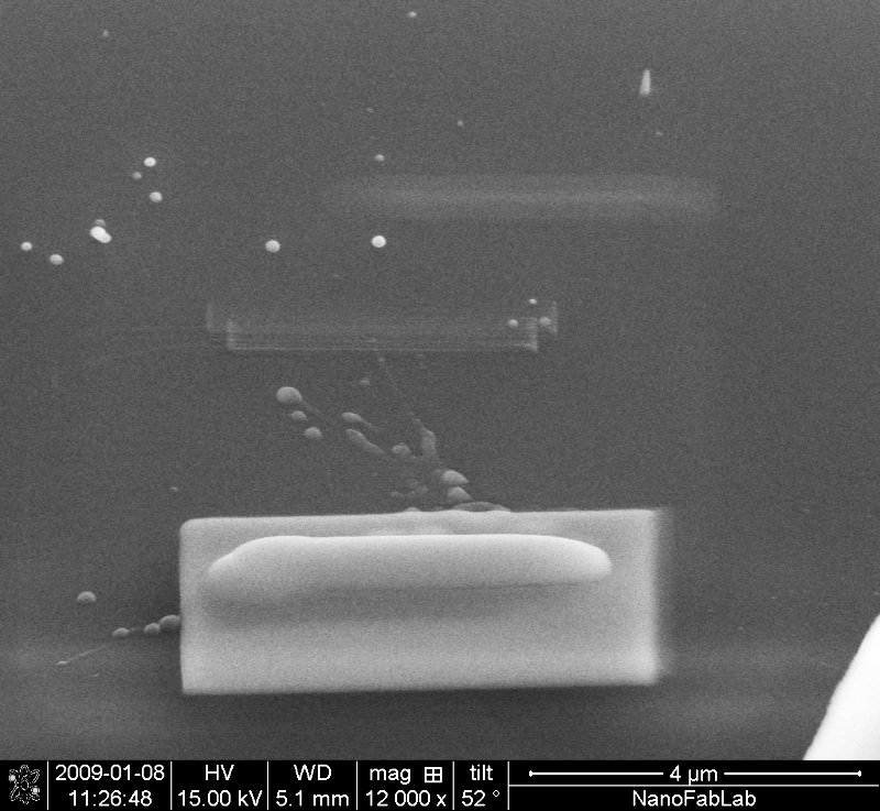
Note the long contamination dots that can be seen from the side in the left
part of the picture. They must have been built during e-beam imaging when
tilt was 52°.
Same area imaged at 52° tilt, note that the long pillars now appear as dots, they are seen head on.
The image area is inside a previously made ASV-session, there are a lot of structures of different heights.
My conclusion is that the 1 pA image is slightly sharper despite that it was not possible to do any optimization with stigmation and focus. However this is uncertain due to more wear of the area during the optimization before collecting the image for the 10 pA aperture.