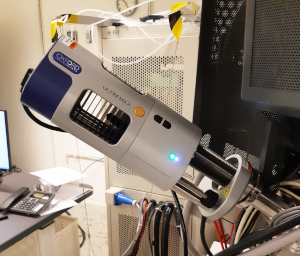
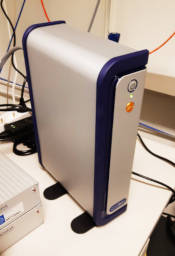
EDX detector in its retracted position and control box.
EDX detector in its retracted position and control box.
Care should be taken when using powder samples to avoid particles to contaminate the EDX detector. Specimens containing particles should be fixated.
The insertion / retraction of the EDX detector is handled form the software via this window:
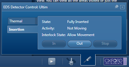
| Here is the EDX detector fully inserted, it is ready to acquire spectra. When you start it should be fully retracted and the "In" button should be enabled. |
Start the Aztec EDX software by clicking the
AZtec link on the desktop.
![]()
First a new project should be created, or an existing project opened. No screen shots yet.
|
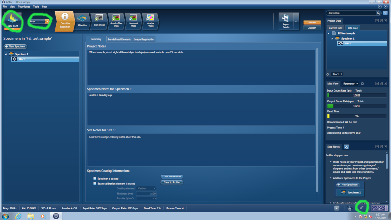
Here is an overivew of the window when a new project has been
created.
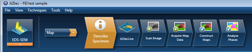
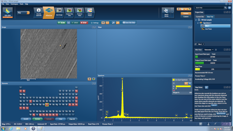
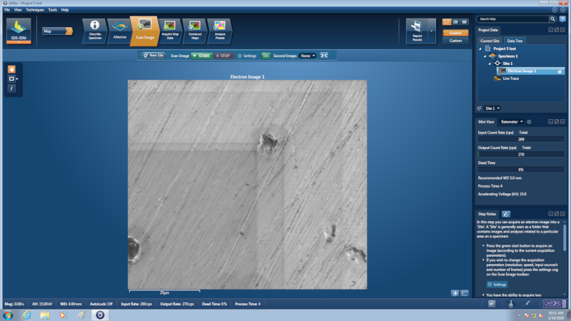
At the lower right encircled in green is the function button to bring up the window for insertion / extraction of the EDX sensor. At the top left is a function selector for the software set to EDS-SEM, this is the only function mode for our system. Next is a drop-down selector for what type of analysis will be done. After that are six step buttons for the different steps that has to be carried out to complete the selected form of analysis. To the left is a column where you can create new specimens within the project. Here is Specimen 1 shown with Site 1 created. In the center are text fields for describing the specimen and site. It is good to fill these out in order to keep track of what has been analyzed. To the right is a Data Tree shown where each part of the analysis is stored. It is possible to go back in the tree to see the previous analysis in the project. Under this is shown the rate meter for the number of photons coming to the detector. It is important that the Dead Time is not exceeding 50%. At the lower right is shown a help text window, where help texts relevent to each analysis step are shown. These are really helpful, please examine these. |
|
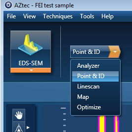
The mode, path and step buttons at the top. Here shown for the
Map path.
Below is the different possible paths shown. This document only describes the Map path. |
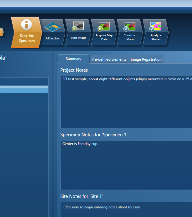
| The summary of the specimen description, first briefly about the whole project, then about the specific specimen, then about the site on the specimen. |
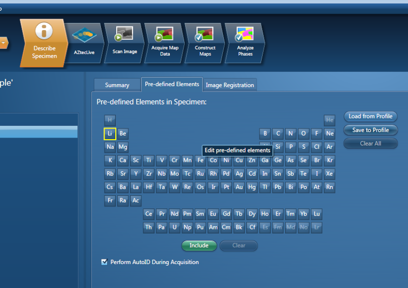
| Under this tab you can specify elements that you know for sure are present in the specimen. |
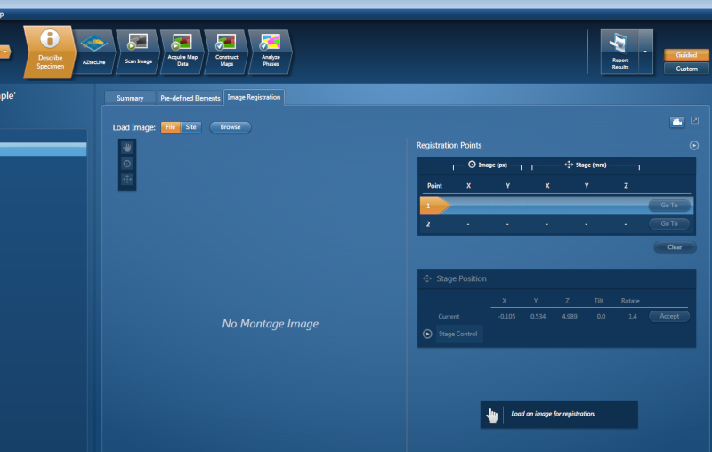
| If you have a picture of the specimen taken earlier, you can load it here, and specify coordinates to match it to the SEM images to be acquired. |
|
Step
AZtecLive is
activated. A SEM image is collected.
The periodic table at the lower left shows the excluded elements in red, this is the default setting. The spectrum is at the lower right, labels for elements are shown at the peaks. |
| Here the spot mode is activated. The sample is a FEI calibration sample, having a Faraday Cup in the center. The cross is placed on the plain surface made of platinum. |
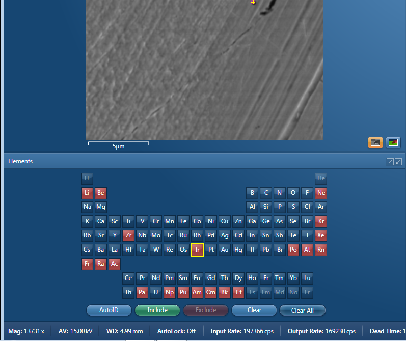
| The excluded elements by default. You can specifically include or exclude elements here. |
|
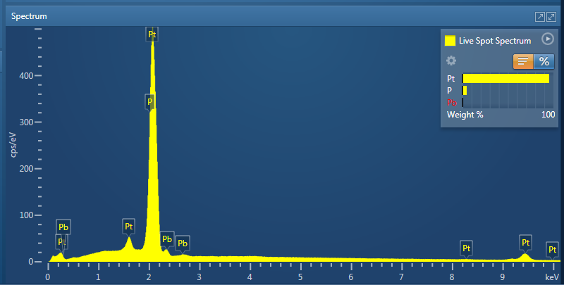
Spectrum showing peaks for Pt, P and Pb. Labels of elements are put
automatically at the peaks.
The spectrum can be zoomed in/out vertically by dragging the pointing device (hold down left button and drag up / down) and zoomed in/out horizontally with the scroll wheel. |
|
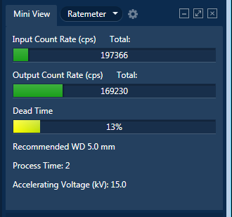
The rate meter to the left, showing Dead Time of 13%, a bit too low,
makes spectrum a bit noisy. Could increase Process Time to 3 or 4,
this is done in Settings next to the Stop button for scanning.
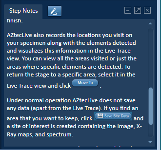
To the right is show an example of the Help texts (Step Notes). These are very helpful, recommended reading. |
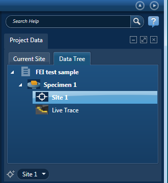
| The Data Tree is updated with the new acquisition. |
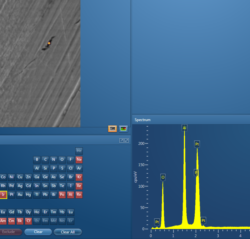
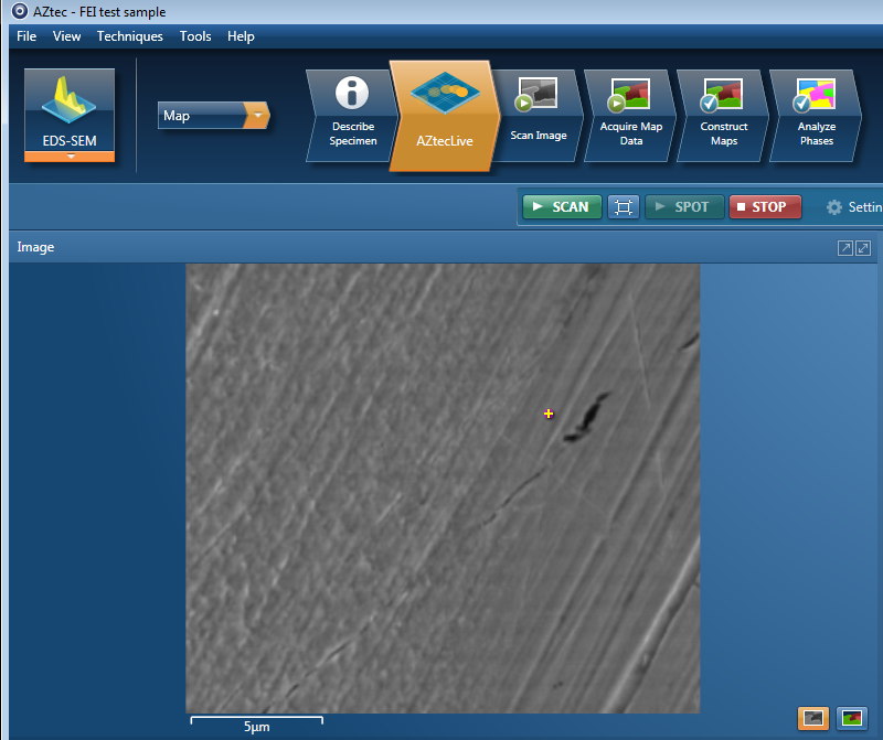
| Here is the measuring point moved to the dark contamination spot and the spectrum is showing oxygen and alumina, indicating a speck of aluminiumoxide. |
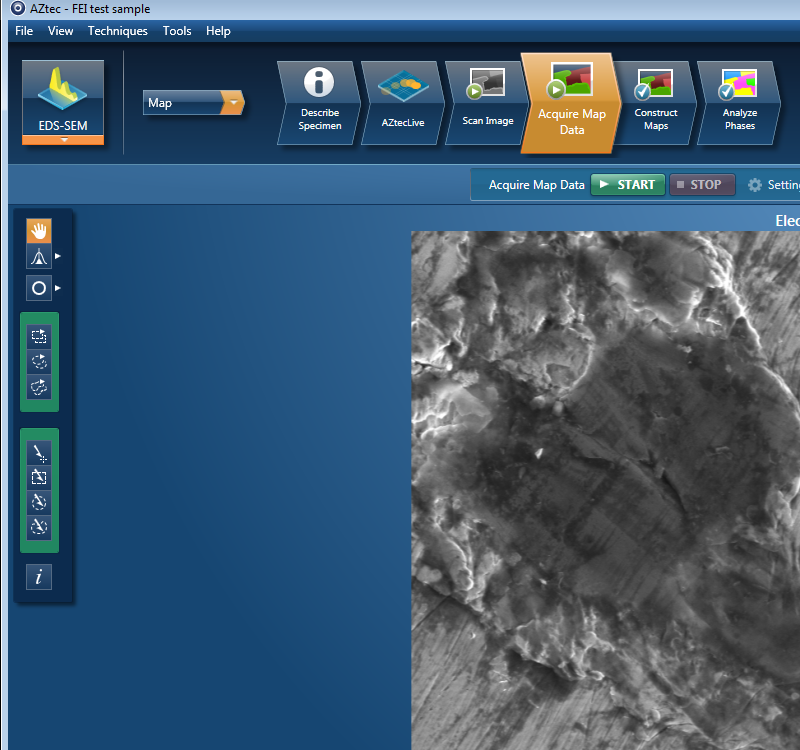
| Next step using function button Scan Image, a SEM image is acquired that will be used as background for element mapping. |
|
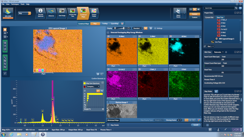
Next step button activated
Acquire Map Data
and an element map can be acquired for the whole image area, or
indicated areas in the image can be used to pinpoint the spectras
collected.
The tools at the left edge are used to encircle interesting areas, the three tools inside the upper green rectangle. To start the acquisition of element map, use the green Start button. |
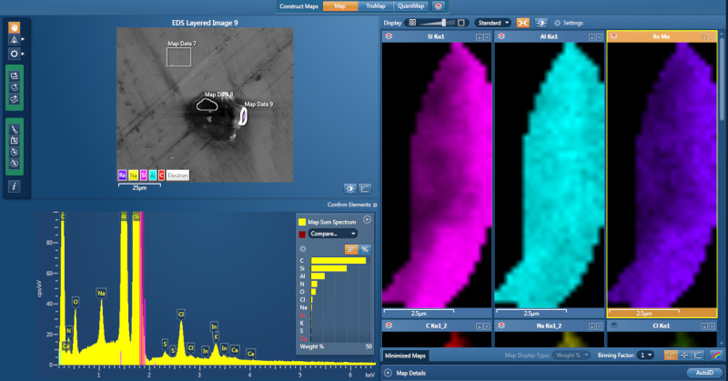
| Here three areas has been encircled, a rectangle and two free form areas. The spectrum and element maps are shown for the high-lighted area (Map Data 9). |
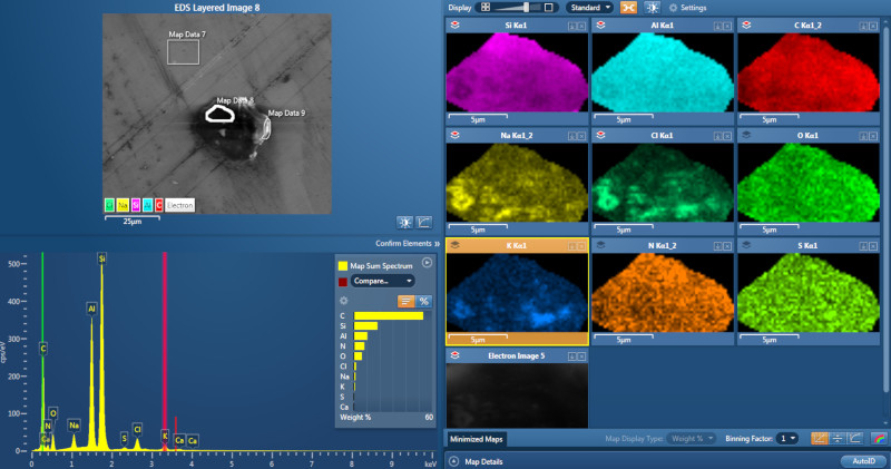
| Here the spectrum and element maps are shown for area Map Data 8. |
| Overview of the whole screen after an element map has been acquired for the image area. The separate maps for each element are shown to the right, and the spectrum below the composite map image. |
|
|
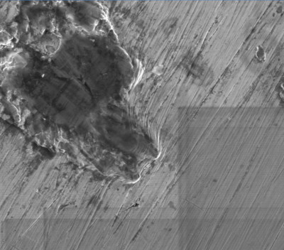
| The SEM image of part of the Pt disc with some contamination. |
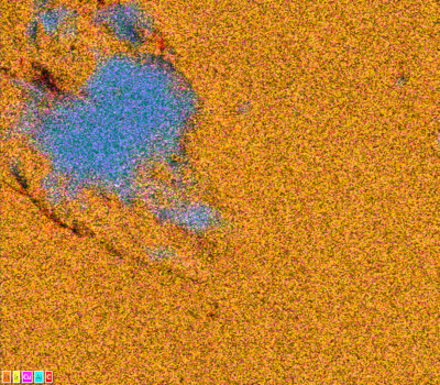
The element map of the same area.
Colors indicate the different elements: Pt = orange, Ir = yellow, Cu = pink, Al = blue, C = red |
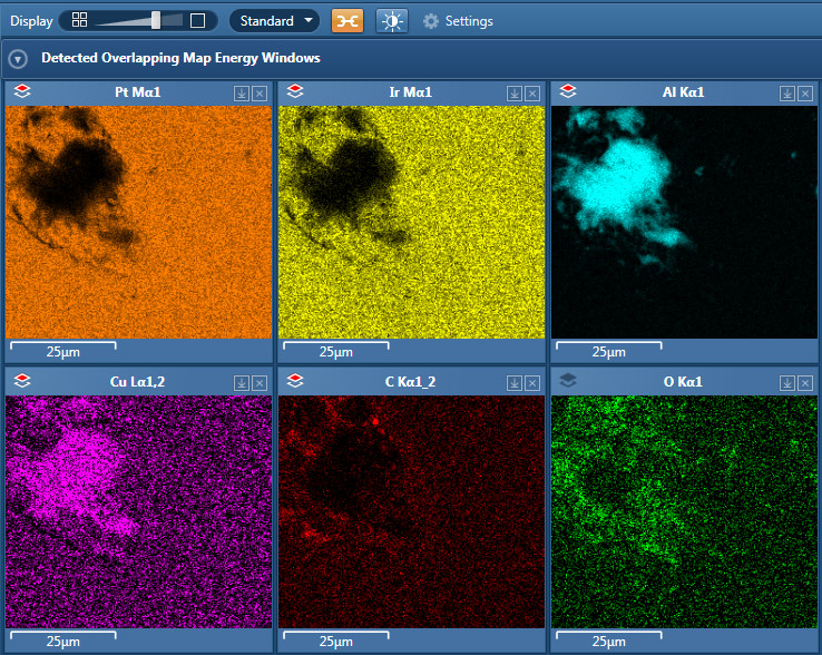
| Here are the separate maps for each element. |
|
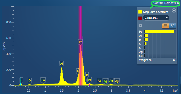
Some elements might be missed in the automatic identification, and
some might be erronenously detected.
In order to correct this there is a function Confirm Elements encircled in green at the upper right corner. |
|
Clicking
Confirm Elements
will take you to a page where elements can be indicated in the
periodic table, and their spectral signatures are shown in the
right hand column. The suggested elements signature is shown in
orange and the acquired spectrum in that range is shown in
yellow.
The indigo line shows the calculated spectrum based on the elements included. The better the fit is with the actual spectrum in yellow, the more complete is the element analysis. You decide which element matches the spectrum peaks best. As you can see three of the four Ag peaks fit well but the fourth does not. Another way is to double click an unlabelled peak in the spectrum and the software will show suggestions for elements in the right hand column. |
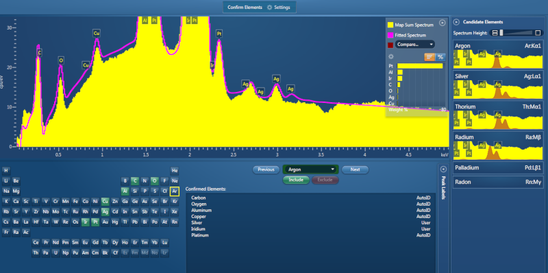
| Here all but one peak was identified by AutoID, the calcium peak was added manually. |
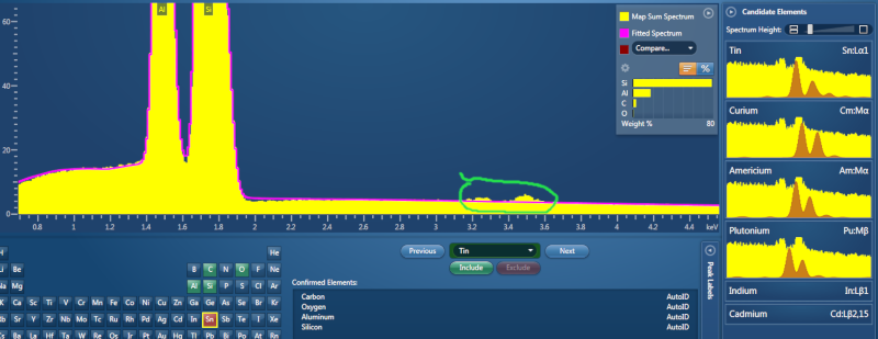
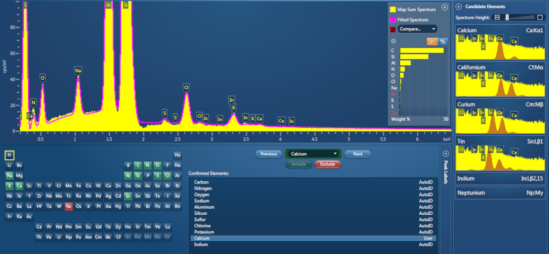
| The peaks encircled in green seem to show up regardless of what elements are in the specimen. Suggestions for Tin, Curium, Americium, Plutonium do not fit well, also the last three are extremely unlikely. |
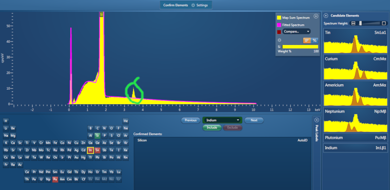
| Here the peaks at about 3.2 and 3.45 kV are also showing up, the specimen is plain Silicon. |
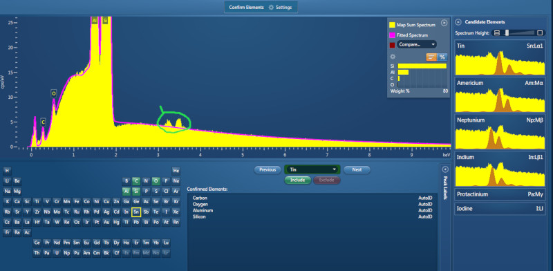
| The same peaks show up here as well, for a different part of the same sample, here with some alumina oxide. |