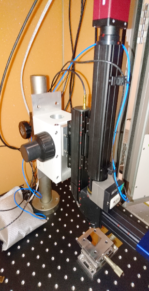
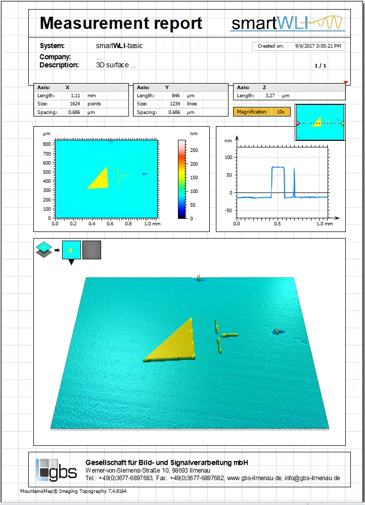
This optical profiler has a fixed objective of 10× magnification, which gives an image field of 1×1 mm.
Responsible: Anders Liljeborg
|
|
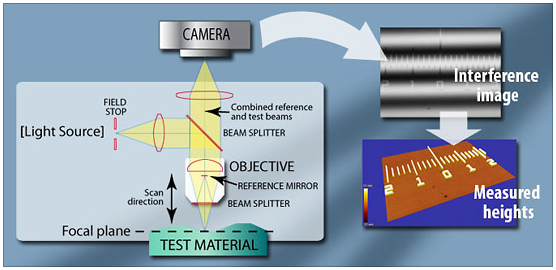
An optical profiler is an interference microscope, and is used to
measure height variations, e.g. surface roughness on reflective
surfaces. The measurement is non-contact as opposed to stylus
profilometers. The measurement is in three dimensions, the height
(Z-axis) is measured over an area of X and Y lateral dimensions.
This optical profiler has a fixed objective of 10× magnification, which gives an image field of 1×1 mm. |
Camera stopped working due to Win10 update
Getting started with MountainsMap software Tutorial 1 Tutorial 2 Tutorial 3 Tutorial 4 Tutorial 5
|
Principle of operation for an optical profiler.
Courtesy Zygo.com |
Here is a quick guide how to operate the optical profiler and collect measurements with it.
1. Wake computer and start software (password provided).
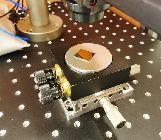
2. Place sample on stage, under objective. To the left are the two levelling knobs. To the right and front are the knobs for moving the sample in X and Y directions.
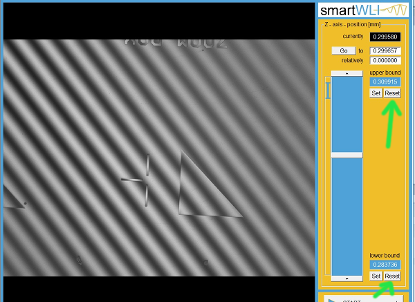
3. Reset the lower and upper bounds of the scanner, and place the slider in the middle of the scan range
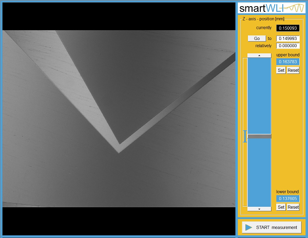
4. Focus on the surface so that you can see interference fringes using the manual focusing knobs on the microscope stand.
5. Level the stage so that the fringes move apart and finally "disappear". This is done with the two knobs on the left side of the upper part of the sample stage.
6. Set the lower and upper bounds by pulling the slider up and down until the interference fringes just disappear from the image.
Click on upper and lower "Set" button to set the respective upper and lower bounds.
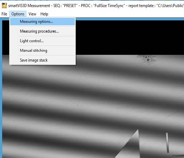
| Bring up the "Measuring Options" from the Options drop-down. |
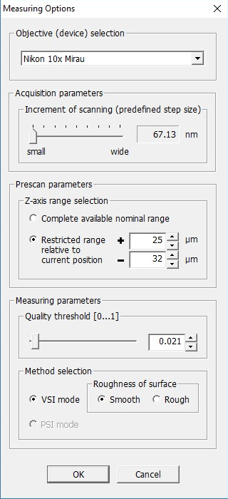
7. Set the scan speed via the "Increment of Scanning". A small value gives a more accurate measurement
8. Quality threshold defines the quality of data that should be kept or discarded. Should be low in most cases (default = 0.03)
9. For most applications in the Nanolab, "VSI mode, Smooth" should be chosen
10. Press "Start Measurement" in the lower right corner.
Measurement
is performed and
transferred to Mountains Maps for analysis and reporting. There is a
preset template for the report, but this can be changed if necessary
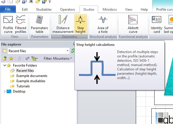
11. Step height can be performed on sections
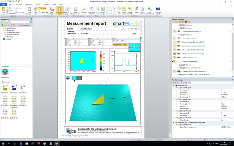
| The complete GUI for the analysis software. To the left tools to put together the measurement report, in the center the report, to the right a list of the measurement steps carried out to generate the report. |
12. Choose section to analyze
13. Level the section to get rid of general slope.
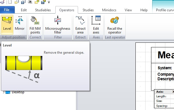
Areas to be used for levelling are selected along a cross-section.
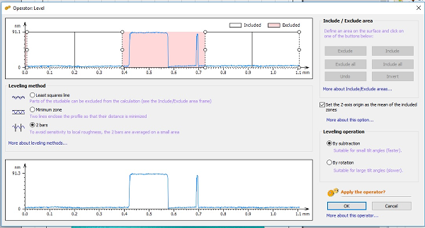
14. Perform step height analysis.
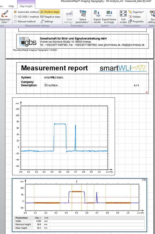
| Result of step height analysis. The orange part of the cross-section are used for the analysis. |
15. To perform roughness analyses on images or sections, press "Parameters Table".
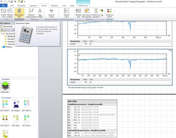
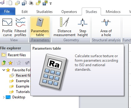
| Generate a "Parameters Table" to measure surface roughness. |
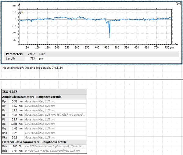
| Resulting table lists several roughness parameters. |
Bring up the properties of the network interface for the camera (not for the internet interface). Click the "Configuration" button, select the "Advanced" tab and set "Jumbo Frames" to maximum value.