Diffractive Optics manufactured w. EBL
Patterning of Tungsten using EBL and negative resist HSQ
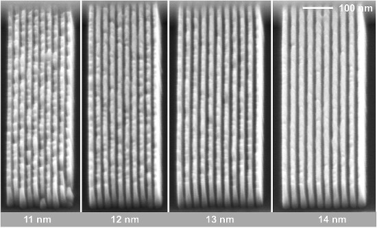
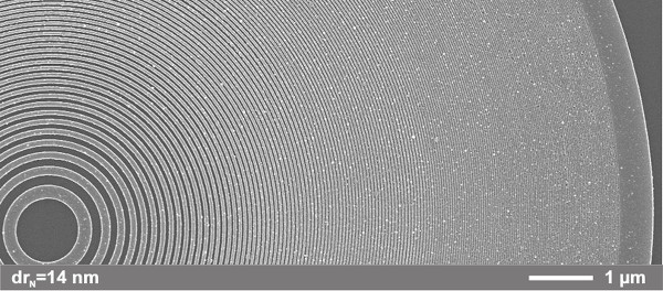
Values indicate half pitch size. 90 nm pattern height.
Courtesy Julia Reinspach, Anders Holmberg,
Biomedical & X-ray Physics, KTH.
High resolution nickel zone plate for soft x-ray microscopy
Outermost part of the zone plate with 16 nm half-pitch, 60 nm high.
Courtesy Julia Reinspach, Anders Holmberg,
Biomedical & X-ray Physics, KTH.
13-nm nickel zone plates fabricated using
cold-developed electron-beam patterned Zep 7000
High-aspect-ratio processing is needed to obtain zone plates with both
high resolution and high diffraction efficiency. To fabricate such
optics we use a tri-layer resist process in combination with
electroplating. Si3 N4 -
membranes are used as substrates
since they have a high x-ray transmission
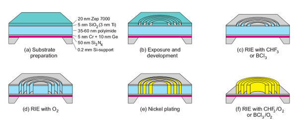
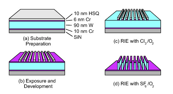
The patterning is performed with 25 keV electron-beam lithography
(Raith 150 system) followed by two steps of reactive ion etching (RIE)
to provide a mold. The mold is filled with the zone-plate material by
electroplating, after which the mold is removed.
Overview image of a nickel zone plate with 14 nm outermost zone width.
The pattern quality is high and uniform over the entire zone plate area.
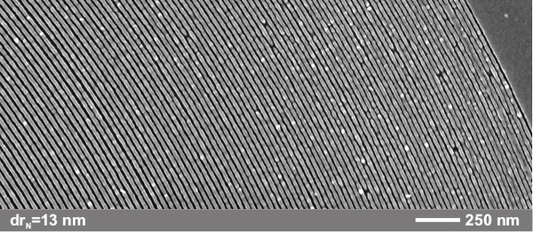
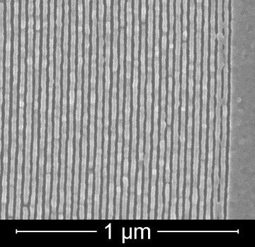
The outer part of a nickel zone plate with 13 nm outermost zone
width.
The nickel thickness is 35 nm.
Cold development was applied in the nanofabrication process and the
resolution improvement enabled the fabrication of zone plates with
outermost zone widths down to 13 nm.
SEM images of electroplated nickel zone plates are shown above. The
zone plate with 15 nm outermost zone width was fabricated using Ti as
hardmask material. For higher resolution SiO2 was used since it
provided a more reproducible pattern transfer.
Courtesy Julia Reinspach, Magnus Lindblom, Anders Holmberg,
Biomedical & X-ray Physics, KTH.
Anders Liljeborg
Nanostructure Physics, KTH.