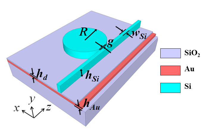
| Fig. 1. Sketch of a hybrid plasmonic microdisk device. |
| Abstract: In this short document, I present a summary of my PhD work which has utilized the Albanova Ebeam Lithography system. It mainly includes two projects: (1) hybrid plasmonic functional devices and (2) perfect-absorber assisted tunable filter. |
| Fig. 1. Sketch of a hybrid plasmonic microdisk device. |
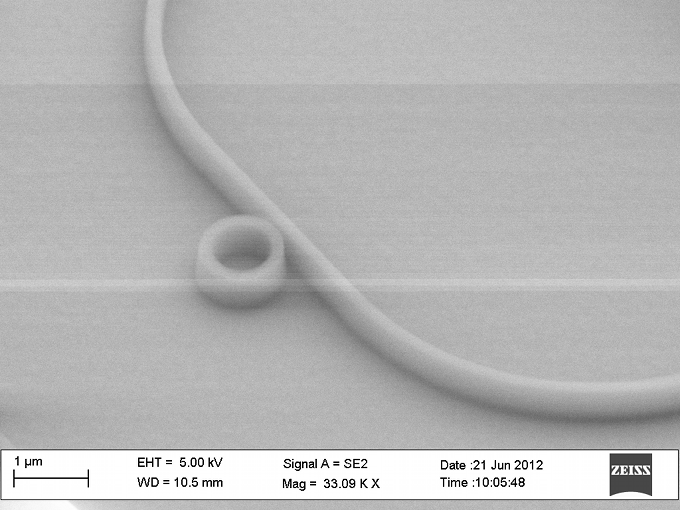
Hybrid plasmonic devices with sizes beyond the diffraction limit of light, including straight waveguides, directional coupler, microdisks, microrings, etc. are experimentally demonstrated, as shown in Fig. 2. The width of the fabricated hybrid plasmonic waveguides is about 170 nm. For directional couplers as shown in Fig. 2 (b) and (c), the gaps between different arms are about 140 nm, 190 nm, 240 nm and 290 nm. The radii of microrings and microdisks are around 500 nm, as shown in Fig. 2 (d) to (h). The gaps between straight access waveguide and resonant cavities are around 50 nm, 100 nm and 150 nm.
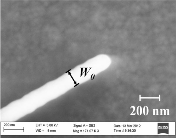
| Fig. 2. Scanning electron microscope of the fabricated hybrid plasmonic device. (a) A straight waveguide with width of w0 ≈ 170 nm. |
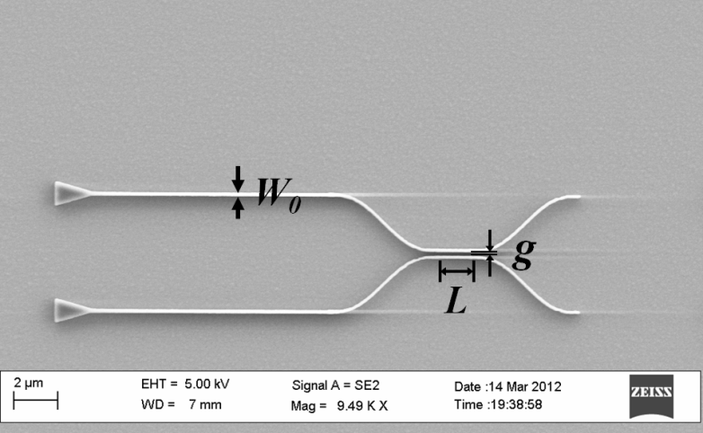
| Fig. 2 (b) A directional coupler with gap of about g ≈ 145 nm. |
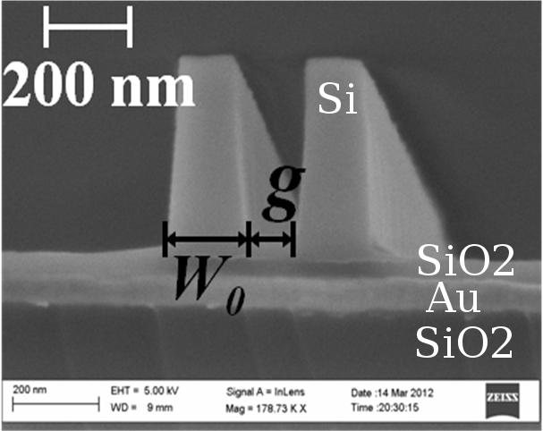
| Fig. 2 (c) Cross section of a directional coupler, where w0 ≈ 170 nm, g ≈ 140 nm. The materials from top to bottom are a-Si, SiO2, Au, and SiO2 respectively. |
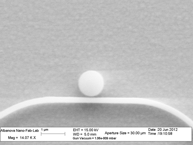
| Fig. 2 (d) Top view of a 1 µm diameter micro-disk, where gap between straight waveguide and micro-disk is about 55 nm. |
| Fig. 2 (e) Tilted view of the disk in (d), where the thick waveguide is polymer. |
| Fig. 2 (f) Tilted view of the disk in (d). |
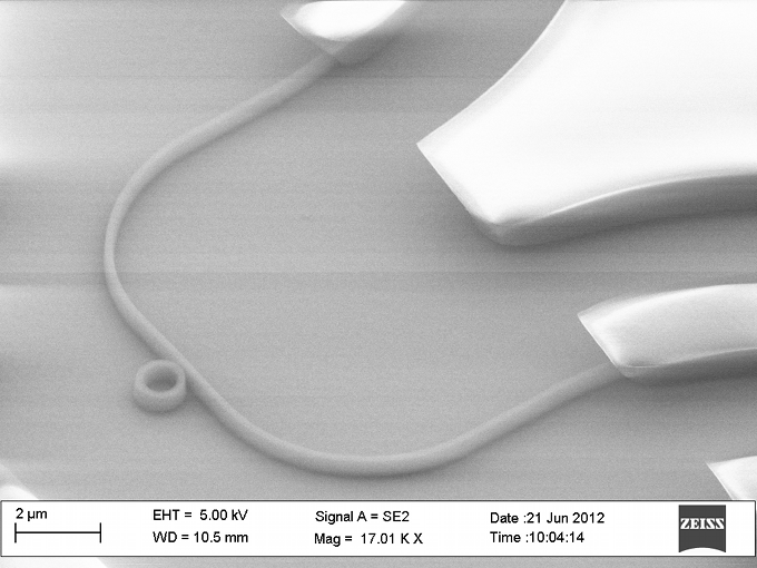
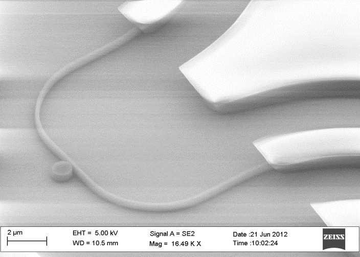
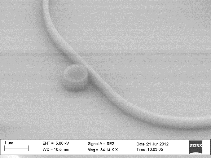
| Fig. 2 (g) Tilted view of a 1 µm diameter micro-ring, where gap between straight waveguide and micro-disk is about 50 nm. |
| Fig. 2 (h) Tilted view of the microring in (g). |
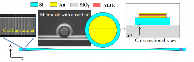
| Fig. 3. Schematics of an absorber-assisted microdisk. |
I did the preliminary exploration of the fabrication, and later Dr. Yuechun Shi took over the fabrication process. Fig. 4 shows the SEM and optical microscope image of the fabricated device.
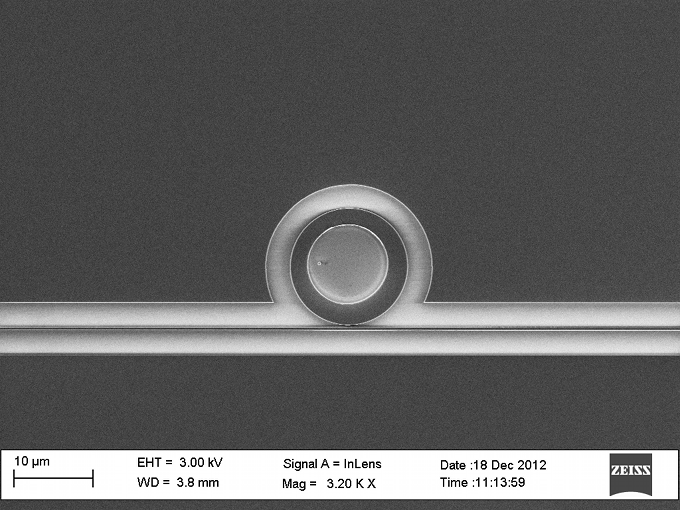
| Fig. 4 (a) SEM image of an absorber-assisted microdisk. The device was fabricated using resist ZEP 520A. The smaller disk on top of a silicon disk was the perfect absorber and it was composed of Au-Al2O3-Au. |
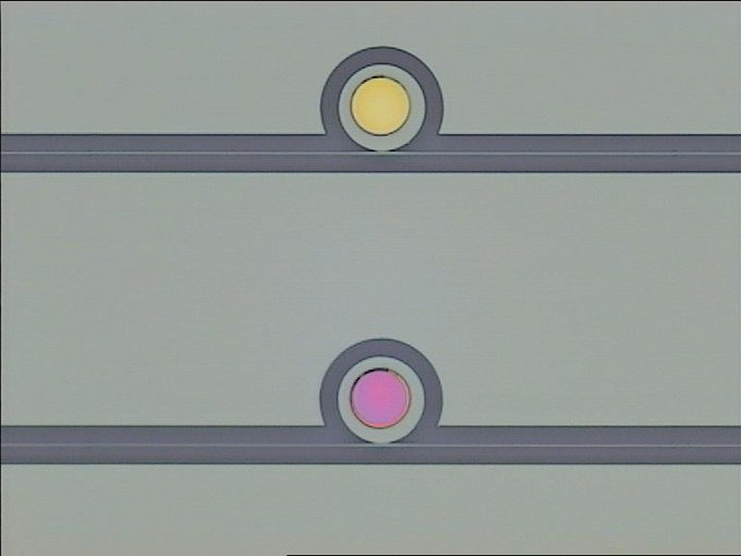
| Fig. 4 (b) Optical microscope image of two fabricated micro-disks in true colors. During the liftoff process, perfect absorber of the bottom device survived; while the absorber of the top device was stripped away; only a gold disk was left. |
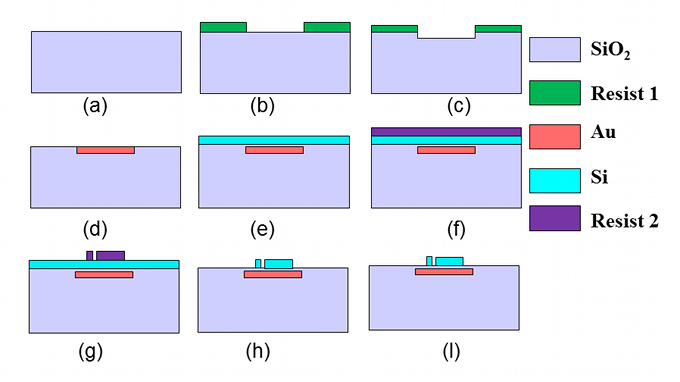
| Fig. 1. Process flow of a hybrid plasmonic device. (a) Deposit SiO2 buffer layer on Si wafer using PECVD. (b) Ebeam litho for metal deposition window. (c) Etch SiO2. (d) Deposit Metal and liftoff. (e) Deposit SiO2 and a-Si. (f) and (g) Ebeam litho to define patterns. (h) Etch a-Si and SiO2. (l) Cleave sample. |
In the process, Electron beam lithos are employed twice to define sub-wavelength scale patterns as shown in Fig. 1 step (b) and (g). In step (b), positive resist ZEP 520A is used to define a window for metal evaporation and liftoff. In step (g), negative resist Ma-N 2403 is used instead to define the patterns of functional devices, e.g. directional couplers, straight waveguides, microrings, etc. The details of the process recipe are shown in Table 1. It's worth mentioning that since multiple lithos are used in the fabrication, markers with known UV coordinates should be defined during the 1:st litho process, which will help make the 3-points alignment for the 2:nd litho. Note that sharp and small markers from the 1:st litho are the pre-requisites of an accurate alignment for the 2:nd litho.
| Step (b) | Step (g) | |
| Step Size | 4 - 10 nm | 4 - 10 nm |
| WF size | 100 µm | 100 µm |
| Resist | ZEP520A | Ma-N 2403 |
| Spin speed | 5500 rpm | 3600 rpm |
| Acceleration Voltage | 25 kV | 25 kV |
| Dose | 60 µAs/cm2 | 110 µAs/cm2 |
| Developer | P-xylene | Ma-D 525S |
| Developing time | 100 sec | 3 min 30 sec |
During the EBL process, there are some practical issues which are worth noticing.
1) The stitching errors. To facilitate the characterization of the devices, the access waveguides are usually more than one writing field of the Ebeam litho system. In order to get a continuous pattern and minimize the propagation loss and reflection ripples, one needs to compensate stitching errors by aligning writing field carefully before exposure. In some critical regions, extra exposure of the stitching regions is necessary to get stitching-error-free patterns.
2) The adhesion between resist and sample. For negative resist Ma-N 2403, the adhesion between sample surface and resist is not very strong, especially when the pattern sizes are small and aspect ratios of height and width are high. Even N2 blow would destroy the patterns in some extreme cases. A possible solution to to address this issue would be using an adhesion promoter before resist spinning in this case.
3) The dose test to minimize proximity effect. The idea dose is sometimes very sensitive to the material of the sample. For a hybrid plasmonic sample with a layer of gold underneath, the dose is relatively smaller than the dose for a sample with silicon substrate. In this regard, one needs to make a series of dose test in order to get high resolution patterns.