Albanova NanoLab - some results
Single Electron Transistor
Two resist layer process:
- bottom layer PMGI SF7 (400nm).
- top layer ZEP 520 diluted (63nm).
Development:
- Pxylol and MF322 (3:2 dill).
Evaporation:
- Aluminum two angle evaporation: 20nm (-14degrees), oxidation, 30nm (+14degrees).
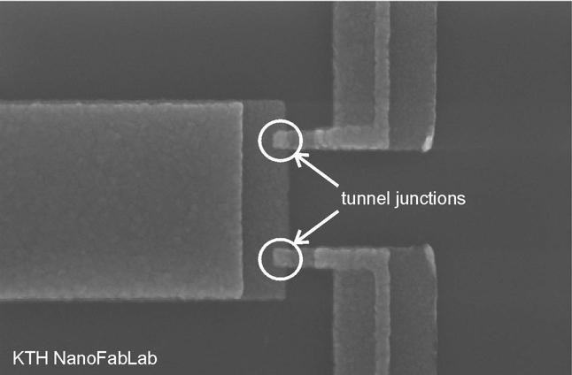
Structure:
- Single electron transistor (SET)
The island in the middle of the image is connected via two 100nm by
100nm tunnel junctions to two electrodes. A capacitively coupled
gate, not shown in this image, can be employed to vary the conductance
of the device.
Albanova NanoLab - some results
Two coupled single electron devices
Two resist layer process:
- bottom layer PMGI SF7 (400nm).
- top layer ZEP 520 diluted (63nm).
Development:
- Pxylol and MF322 (3:2 dill).
Evaporation:
- Aluminum two angle evaporation: 20nm (-14degrees), oxidation, 30nm (+14degrees).
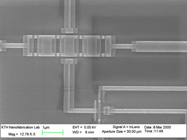
Structure:
- Two capacitively coupled single electron devices
The bottom structure is a simple single electron transistor (SET). The
central island is capacitively coupled to an external gate electrode.
The island of the lower SET extends all the way to the second device,
and couples capacitively to the central island of the series
combination of 4 DC SQUIDs. A second external gate couples also the
center island.
Volker Schöllmann
Webmaster
Albanova NanoLab