Ebeam Litho, Yiting Chen

Some results from Ebeam lithography done by Yiting Chen at Albanova Nanofabrication Facility


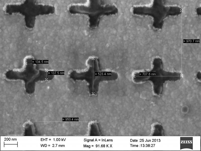
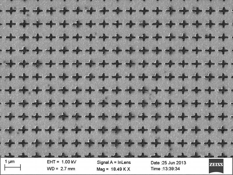
This is a plasmonic quarter-wave plate, with subwavelength cross-shaped appertures in the 60 nm thick gold film on top of silicon substrate. Due to the difference between the lengthes of the arms of the cross, the phase difference is introduced to the orthogonal polarizations of the normal incident light. By carefully design the lengthes of the arms of the cross, a quarter-wave plate in particular wavelength can be realized.

For example, when the lengths of the arms are 511 nm and 680 nm, respectively, and the width of the arms is 100 nm, it will be a quarter-wave plate at 1550 nm, which means the transmitted light of a linearly polarized incident light will be circularly polarized light, and vice versa.

The sample are fabricated by EBL with negative resist MaN 2403.

Aperture: 10 µm
Write Field: 100 × 100 µm
Step size: 6 nm
Voltage: 25 kV
Total size of the pattern: 100 µm

FBMS mode was not used.


A detail of the pattern with measures.


Plasmonic metamaterial absorber at infra-red regime

A wide-angle Metal-Insulator-Metal (MIM) plasmonic absorber at 1140 nm, with gold disks at honeycomb lattice on top the alumina and gold film. The thicknesses of the gold, alumina and gold layers from top to bottom are 30 nm, 28 nm and 80 nm, respectively. The absorber almost has perfect absorption at around 1140 nm. The absorption wavelength is tunable by altering the diameter of the gold disks.

Details can be found in this paper (pdf)

Aperture: 10 µm
Write Field: 100 × 100 µm
Step size: 6 nm
Voltage: 25 kV
Total size of the pattern: 100 µm

FBMS mode was not used.


Anders Liljeborg Nanostructure Physics, KTH.