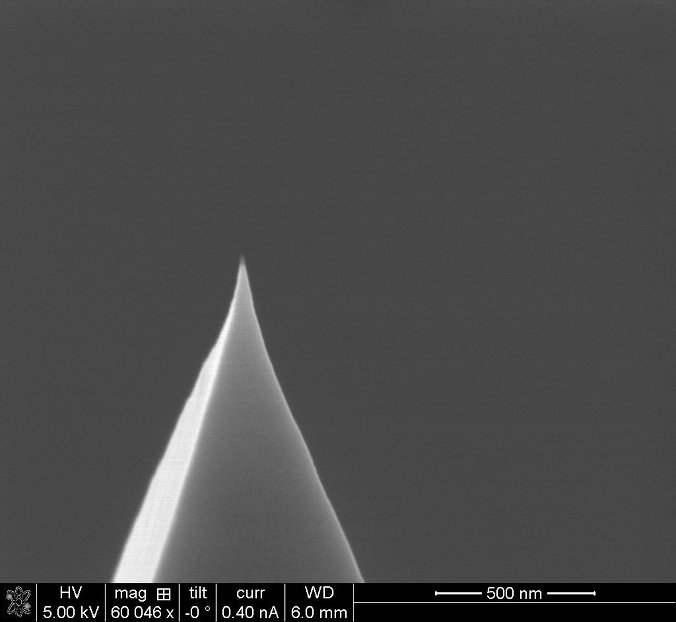
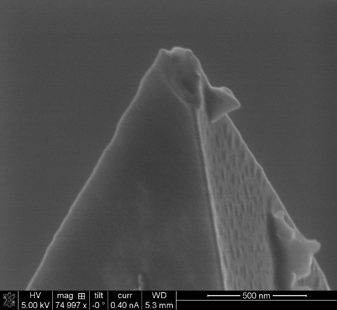
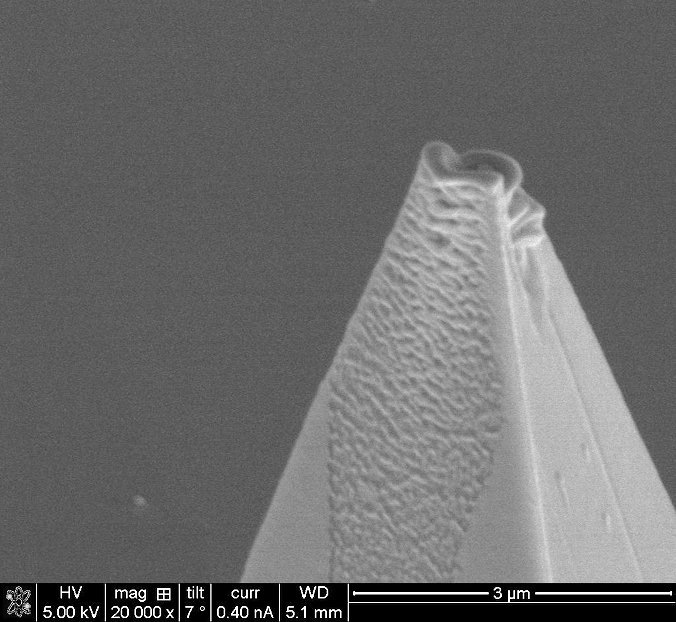
| A tip used only once, imaged in immersion mode. Tip is Tap300Al-G from Budget Sensors, 300 kHz, 40 N/m. |
| A tip used only once, imaged in immersion mode. Tip is Tap300Al-G from Budget Sensors, 300 kHz, 40 N/m. |
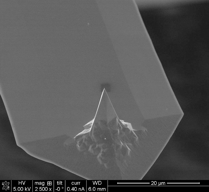
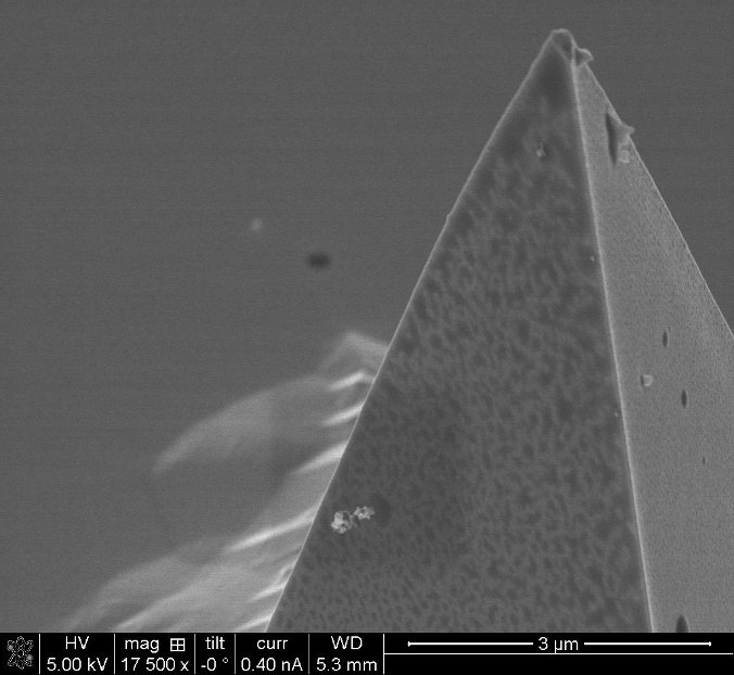
| Overview of same tip. |
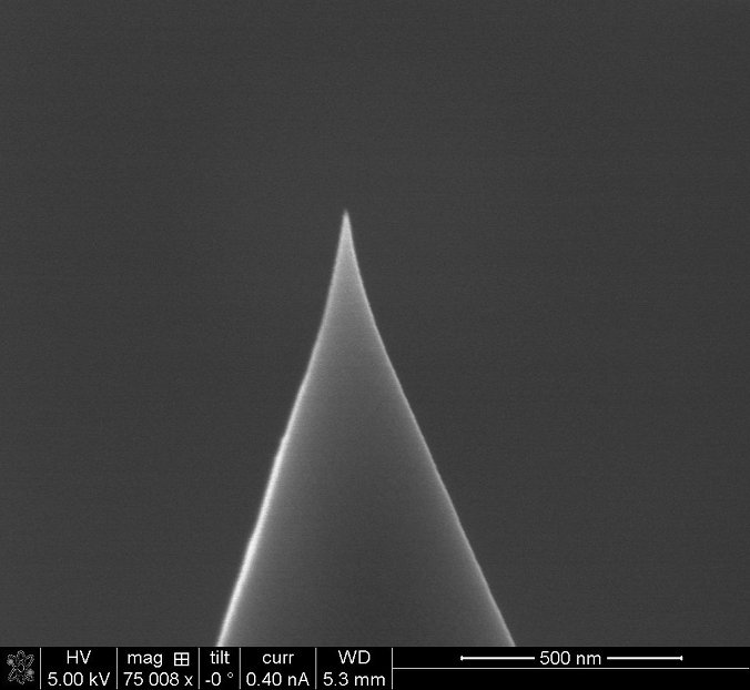
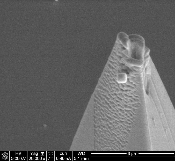
| An unused tip of same type: Tap300Al-G, Budget Sensors, 300 kHz, 40 N/m. |
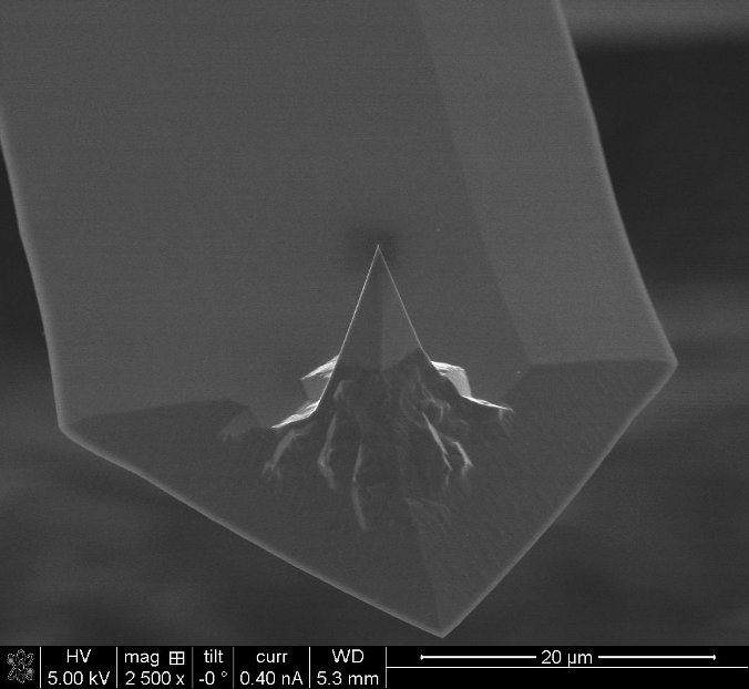
| Overview of same tip. |
|
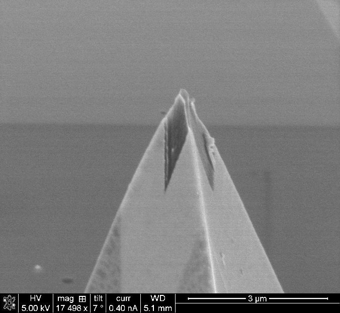
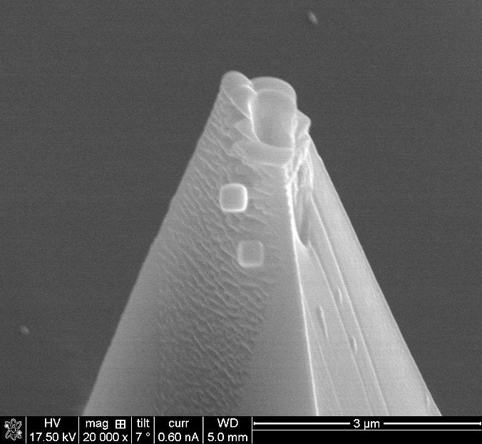
Very old tip that came with the used Veeco Dimension 3100 system
from TFE, Linköping. Tip is for electrostatic force measurements,
type EFM-16, coating Ptlr5, made by Nanosensors, Germany.
The tip is probably used, not very sharp. |
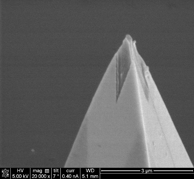
| Close up of tip. |
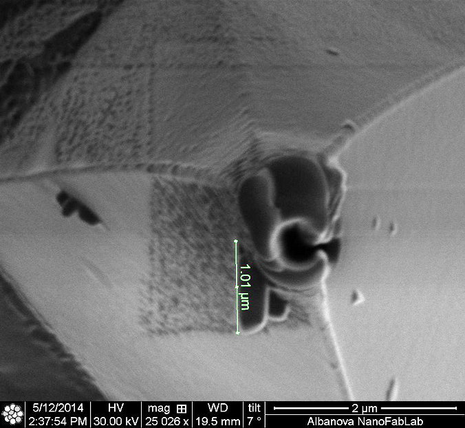
| The tip after it has been imaged with the ion-beam for a while, ion current 10 pA, 30 kV. |
| Here a trial with smallest ion current (1 pA) to deposit a small pillar of platinum, nominal diameter 50 nm. No deposition can be seen. |
| Here ion current has been increased to 100 pA, and a one micron dot was deposited. Not good at all. It seems the ion-beam is deposition the platinum but at the same time also milling it away. |
|
A couple of more trials with ion-beam Pt-deposition at 100 pA has
changed the
shape of the tip, compare with previous picture.
Then E-beam deposition is used, immersion mode, both for deposition and imaging. A small square with a nominal height of 5 µm can be seen below the top. |
| Switched E-beam voltage to 17 kV, and did same small square, below the first one. |
| Here a image taken with ion-beam, 10 pA, for a quick look at how the ebeam deposition worked. The length of the deposited pillar is about one micron, far from the nominal value of five microns. |