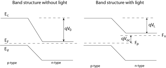
Shining a laser on a p-n junction or any device based upon semiconductor doping causes generation of electron-hole pairs. These electron-hole pairs significantly affect the minority carrier concentration, hence the Fermi energy level and the width of the depletion region. See Figure 1 and Figure 2.
Figure 1: Band structure change with light
The width of the depletion region is
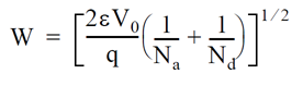
where e is the permittivity, V0 the contact potential, q the electric charge and Na and Nd the concentration of acceptors (p-type) and donors (n-type). The open circuit potential, Voc, is
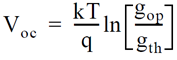
where gop is the optical yield of electron-hole pairs and gth is the thermal yield of electron-hole pairs. The voltage when light is applied is

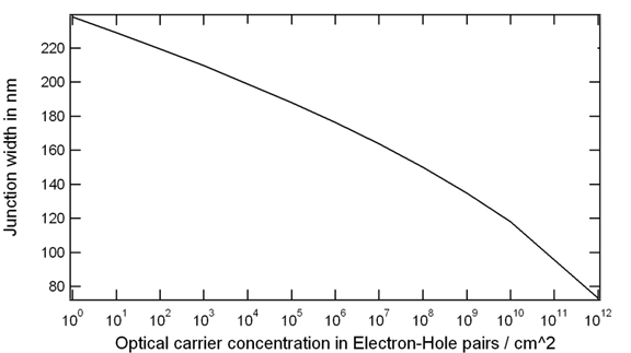
Figure 2: p-n junction width as a function of optical carrier concentration
| www.bruker.com | Bruker Corporation |
| www.brukerafmprobes.com | 112 Robin Hill Rd. |
| nanoscaleworld.bruker-axs.com/nanoscaleworld/ | Santa Barbara, CA 93117 |
| Customer Support: (800) 873-9750 | |
| Copyright 2010, 2011. All Rights Reserved. |